Frequently Asked Questions about Data Converters
Abstract: This article answers most of the common questions regarding data converters. Presented in a classic FAQ format, it addresses topics including: defining an ADC and DAC, and understanding their principal functions; the Nyquist, effects of charge injection; techniques for digital filtering; interfacing to a serial port, I2C interface, and SPI interface; bit banging; MICROWIRE interface; PCB (PC-board) layout tips and guidelines; grounding tips; bypass capacitor(s)' effect on performance; debugging ADC accuracy; and debugging noisy measurements.
Check the list of questions or the list of keywords below.
Questions
Introductory Questions
What Is an ADC (Analog-to-Digital Converter)?
What Is a DAC (Digital-to-Analog Converter)?
How Does an Algorithmic ADC Work?
How Does a Pipeline ADC Work?
How Does a Delta-Sigma (or Sigma-Delta) ADC Work?
How Does a Flash ADC Work?
How Does a SAR (Successive-Approximation-Register) ADC Work?
How Does a Dual-Slope Integrating ADC Work?
Intermediate Questions
What Is the Nyquist Limit?
Why Does the ADC Disrupt the Signal that It Is Measuring?
What Techniques Are Used for Digital Filtering?
When Should I Use a Balun?
Applications
Can I Connect a Serial ADC to My Computer's Serial Port?
Can I Get a "Smart" ADC?
What Is the SPI? Interface?
My Microcontroller Has No SPI Interface. Is There a Circuit to Convert SPI to Parallel?
How Can I Debug (or Probe) an SPI Interface?
What Is Bit-Banging?
My Microcontroller Has No SPI Interface. Can I Use Bit-Banging?
What Is the MICROWIRE? Interface?
What Is the I2C Interface?
My Microcontroller Has No I2C Interface.Can I Use Bit-Banging?
PCB (PC-Board) Layout Guidelines
Do You Have Any General Circuit-Layout Tips?
Do You Have Any Circuit-Layout Tips for ADCs?
Do You Have Any Grounding/Ground Plane Tips?
Can the 0.1μf Bypass Capacitors Be Eliminated?
How Can I Model the Real-World Effects of PCBs?
Debugging and Diagnostics
Why Am I Not Getting the Specified Accuracy from My ADC?
Why Is the Output Code Stuck at All Ones?
Why Are the ADC Measurements Noisy?
I Noticed Noise from the MAX194/MAX195. How Do I Get Rid of It?
Keywords
A/D
What Is an ADC (Analog-to-Digital Converter)?
ADC
What Is an ADC (Analog-to-Digital Converter)?
Algorithmic
How Does an Algorithmic ADC Work?
Bit-Banging
What Is Bit-Banging?
My Microcontroller Has No SPI Interface. Can I Use Bit-Banging?
My Microcontroller Has No I2C Interface. Can I Use Bit-Banging?
Capacitors
Can the 0.1μf Bypass Capacitors Be Eliminated?
Charge-Balancing
How Does a SAR (Successive-Approximation-Register) ADC Work?
COM
Can I Connect a Serial ADC to My Computer's Serial Port?
CPHA
What Is the SPI Interface?
CPOL
What Is the SPI Interface?
D/A
What Is a DAC (Digital-to-Analog) Converter?
DAC
What Is a DAC (Digital-to-Analog) Converter?
Delta Sigma
How Does a Delta-Sigma (or Sigma-Delta) ADC Work?
DSP
What Techniques Are Used for Digital Filtering?
Dual Slope
How Does a Dual-Slope Integrating ADC Work?
FFT
What Techniques Are Used for Digital Filtering?
FIR
What Techniques Are Used for Digital Filtering?
Flash
How Does a Flash ADC Work?
I2C
What Is the I2C Interface?
My Microcontroller Has No I2C Interface. Can I Use Bit-Banging?
IIR
What Techniques Are Used for Digital Filtering?
Layout
Do You Have Any General Circuit-Layout Tips?
Do You Have Any Circuit-Layout Tips for ADCs?
Do You Have Any Grounding/Ground Plane Tips?
How Can I Model Real-World Effects of PCBs?
MAX104
How Does a Flash ADC Work?
MAX109
How Does a Flash ADC Work?
MAX1213N/MAX1214N/MAX1215N
How Does a Pipeline ADC Work?
MAX1280
How Does a SAR (Successive-Approximation-Register) ADC Work?
MAX132
How Does a Dual-Slope Integrating ADC Work?
MAX1400
How Does a Sigma-Delta (or Delta-Sigma) ADC Work?
MAX1460
Can I Get a "Smart" ADC?
MAX194
I Noticed Noise from the MAX194/MAX195. How Do I Get Rid of It?
MAX195
My Microcontroller Has No SPI Interface.Is There a Circuit to Convert SPI to Parallel?
I Noticed Noise from the MAX194/MAX195. How Do I Get Rid of It?
MAX7651
Can I Get a "Smart" ADC?
MAX19515/MAX19516/MAX19517
How Does a Pipeline ADC Work?
MAX19586/MAX19588
How Does a Pipeline ADC Work?
Microcontroller
Can I Get a "Smart" ADC?
MICROWIRE
What Is the MICROWIRE Interface?
MISO
What Is the SPI Interface?
Modeling
How Can I Model Real-World Effects of PCBs?
Modulator
How Does a Sigma-Delta (or Delta-Sigma) ADC Work?
MOSI
What Is the SPI Interface?
Noise
Why Are the ADC Measurements Noisy?
I Noticed Noise from the MAX194/MAX195. How Do I Get Rid of It?
Parallel
My Microcontroller Has No SPI Interface. Is There a Circuit to Convert SPI to Parallel?
Parasitic
How Can I Model Real-World Effects of PCBs?
Pipeline
How Does a Pipeline ADC Work?
Production
Can the 0.1μf Bypass Capacitors Be Eliminated?
How Can I Model Real-World Effects of PCBs?
Prototype
How Can I Model Real-World Effects of PCBs?
RS-232
Can I Connect a Serial ADC to My Computer's Serial Port?
SAR
How Does a SAR (Successive-Approximation-Register) ADC Work?
SCLK
What Is the SPI Interface?
Serial
Can I Connect a Serial ADC to My Computer's Serial Port?
What Is the SPI Interface?
My Microcontroller Has No SPI Interface. Is There a Circuit to Convert SPI to Parallel?
How Can I Debug (or Probe) an SPI Interface?
My Microcontroller Has No SPI Interface. Can I Use Bit-Banging?
What Is the MICROWIRE Interface?
What Is the I2C Interface?
Sigma Delta
How Does a Sigma-Delta (or Delta-Sigma) ADC Work?
"Smart" ADC
Can I Get a "Smart" ADC?
SPI
What Is the SPI Interface?
My Microcontroller Has No SPI Interface. Is There a Circuit to Convert SPI to Parallel?
How Can I Debug (or Probe) an SPI Interface?
My Microcontroller Has No SPI Interface. Can I Use Bit-Banging?
Successive Approximation Register
How Does a SAR (Successive-Approximation-Register) ADC Work?
Troubleshooting
How Can I Debug (or Probe) an SPI Interface?
Why Is the Output Code Stuck at All Ones?
Why Are the ADC Measurements Noisy?
I Noticed Noise from the MAX194/MAX195. How Do I Get Rid of It?
Wavelet
What Techniques Are Used for Digital Filtering?
Introductory Questions
This section includes general introductory questions about ADCs.
References
Data Converters
Principles of Data Conversion System Design
Behzad Razavi
IEEE? Press, 1995
ISBN 0-7803-1093-4
IEEE order number: PC4465
The Art of Electronics (2nd Edition)
Paul Horowitz, Winfield Hill
Cambridge University Press, 1989
ISBN 0-5213-7095-7
What Is an ADC (Analog-to-Digital Converter)?
An analog-to-digital converter (also known as an ADC or an A/D converter) is an electronic circuit that measures a real-world signal (such as temperature, pressure, acceleration, and speed) and converts it to a digital representation of the signal.
An ADC compares the analog input voltage to a known reference voltage and then produces a digital representation of this analog input. The output of an ADC is a digital binary code. By its nature, an ADC introduces a quantization error, which is simply the information that is lost. This error occurs because there are an infinite number of voltages for a continuous analog signal, but only a finite number of ADC digital codes. Therefore, the more digital codes that the ADC can resolve, the more resolution it has and the less information lost to quantization error.
BACK TO QUESTIONS
What Is a DAC (Digital-to-Analog Converter)?
A digital-to-analog converter (also known as a DAC or a D/A converter) is an electronic circuit that converts a digital representation of a quantity into a discrete analog value. The input to the DAC is typically a digital binary code. This code, along with a known reference voltage, results in a voltage or current at the DAC's output. The word "discrete" is very important to understand, because a DAC cannot provide a continuous-time output signal. Rather, it provides analog "steps." The steps can be lowpass filtered to obtain a continuous signal. By increasing the resolution of the DAC, the number of discrete steps is increased and the step size is reduced (which reduces the quantization error). This operation results in a signal that closer approximates a continuous-time signal.
BACK TO QUESTIONS
How Does an Algorithmic ADC Work?
An algorithmic ADC is used in high-resolution and low-power applications. It operates based on comparisons between the ADC's reference voltage and the input signal. In this architecture, the reference is constant. The input signal changes in the range of zero to the reference voltage. In this method, the input signal is doubled and compared to the reference. As long as the input signal is less than the reference, the output is set to zero. The input signal is multiplied by 2 and is compared to the reference until it exceeds the reference. Then the output is set to 1 and the reference is subtracted from the input signal. The process can be repeated to achieve higher resolution.
BACK TO QUESTIONS
How Does a Pipeline ADC Work?
The pipelined ADC has become the most popular ADC architecture for sampling rates from a few Msps up to more than 250Msps. Resolution is in the range of 8 bits at the faster sampling rates, up to 16 bits at the lower sampling rates. In this architecture, the converter is multistage and accepts a signal before completing the conversation of the previous signal. In this method, one stage processes data received from the previous stage during a clock cycle. At the end of the clock cycle, the output of a given stage is passed to the next stage using T/H and new data is fed to the previous stage.
Examples of pipeline converters are the dual channel MAX19515 (10-bit, 65Msps), and MAX19516 (10-bit, 100Msps), MAX19517 (10-bit, 130Msps). The MAX19586 is a high-dynamic-range, 16-Bit, 80Msps ADC with -82dBFS noise floor. At 100Msps, the MAX19588 offers an industry-leading -82dBFS noise floor for a new generation of high-sensitivity equipment. Maxim also offers a pin-compatible family of 170Msps to 250Msps, 12-/10-/8-Bit ADCs with the industry's best dynamic performance: the MAX1213N, 12-Bit, 170Msps for broadband applications; the MAX1214N, 12-Bit, 210Msps for broadband applications; and the MAX1215N, 12-bit, 250Msps with industry's highest SNR and SFDR at high input frequencies.
Refer to the application note 1023, "Understanding Pipelined ADCs."
BACK TO QUESTIONS
How Does a Sigma-Delta (or Delta-Sigma) ADC Work?
Sigma-delta converters offer high resolution, high integration, and low cost which makes them a good choice for applications such as process control and weighing scales.
Refer to application note 1870, "Demystifying Sigma-Delta ADCs."
BACK TO QUESTIONS
How Does a Flash ADC Work?
A flash ADC is also called a "parallel encoder." The key advantage of this architecture is very fast conversion times. The main disadvantage is high power consumption. A flash ADC is suited for very-high-speed, low-resolution applications. This architecture becomes prohibitively expensive for higher resolutions. The MAX104 is an example of a flash ADC. The MAX109 is an RF/IF sampling, 8-bit, 2.2Gsps flash converter with 44dB SNR beyond Nyquist.
Refer to the application note 810, "Understanding Flash ADCs."
For additional information, refer to The Art of Electronics.
BACK TO QUESTIONS
How Does a SAR (Successive-Approximation-Register) ADC Work?
Refer to the application note 1080, "Understanding SAR ADCs."
For additional information, refer to The Art of Electronics or to the Motorola? M68HC11 Reference Manual (Chapter 12), a microcontroller reference manual from Motorola.
BACK TO QUESTIONS
How Does a Dual-Slope Integrating ADC Work?
A dual-slope integrating ADC is best suited for low-speed applications where good power-supply rejection is desired. The MAX132 is an example of a dual-slope ADC.
See application note 1041, "Understanding Integrating ADCs" for more information.
For additional information, refer to The Art of Electronics.
BACK TO QUESTIONS
Intermediate Questions
This section covers more involved ADC issues.
What Is the Nyquist Limit?
The Nyquist limit is defined as half of the sampling frequency. The Nyquist limit sets the highest frequency that the system can sample without frequency aliasing. In a sampled data system when the input signal of interest is sampled at a rate slower than the Nyquist limit (fIN > 0.5fSAMPLE), the signal is effectively "folded back" into the Nyquist band. The signal thus appears to be at a lower frequency than it actually is. This unwanted signal is indistinguishable from other signals in the desired frequency band (fSAMPLE/2).
For example, if your system samples the ADC at 2.048kHz, the Nyquist limit for that system is 1.024kHz. If an input signal is applied at 2.56kHz, the input signal is indistinguishable from a 0.512kHz signal (2.56kHz–2.048kHz) due to frequency aliasing. No amount of clever digital signal processing can restore the information lost from frequency aliasing. The only way to know what you have sampled is to physically restrict the input bandwidth prior to sampling.
To minimize sampling errors, you should sample at a rate much higher than two times the Nyquist limit. For example, a 1kHz signal sampled at 2kHz has only two samples per cycle. If you sample precisely at the signal's highest and lowest points, you can measure its frequency and amplitude. However, in many systems you have no guarantee where you are sampling. In the above example, if you sample at the zero crossings of the sine wave, the digitized result will appear to be a DC signal. Thus both the digitized frequency and amplitude information will be incorrect.
Ideally, you should set the sample rate at least five to 10 times the maximum signal frequency of interest. Use a small, lowpass, analog RC input filter to prevent unwanted high-frequency energy from being measured.
Even if you do not explicitly include an RC filter, there is usually some series resistance between the signal source and the ADC, and some capacitance between the ADC input and ground. While this forms an RC filter, often the time constant is so small that it actually does not provide any helpful filtering. For example, with R = 100Ω and C = 10pF, the time constant is 1ns, giving a -3dB cutoff frequency of 159MHz.
Frequency aliasing can be used as an advantage. The effect is similar to tuning a superheterodyne radio receiver. If the spectrum of interest is at a high frequency (not including DC), then it may be possible to digitize the input signal with a significantly slower sample rate than the frequencies of interest. This technique is generally known as "undersampling."
BACK TO QUESTIONS
Why Does the ADC Disrupt the Signal that It Is Measuring?
Some ADCs sample the input signal continuously; other ADCs sample at specific times. Any ADC that uses a track/hold buffer must periodically connect its track/hold capacitor to the input signal, an action that causes a small inrush current. The track/hold capacitor requires time to charge to the correct voltage. This is referred to as "charge injection."
This disruption is usually negligible, because the track/hold capacitor requires such a small charge current and because it quickly charges to the correct voltage. However, if the input impedance is large or the signal source responds slowly to minor disruptions, the system may not settle to the desired accuracy within the allocated sampling time.
This is how to determine if a system is disrupted by charge injection:
- Connect an oscilloscope (channel 1) to the analog input of the ADC.
- Connect the oscilloscope (channel 2) to the conversion start or chip-select signal of the ADC.
- Make the ADC acquire data at a steady rate.
- Trigger the oscilloscope on channel 2.
- Check the ADC's input signal for voltage disruption. Consult the data sheet to determine when sampling begins.
One way to solve this type of problem is to select an op-amp buffer that has sufficient settling time. How fast is "sufficient"? That depends on the accuracy required by your system.
Another solution is to increase the ADC's acquisition time (the time allowed to measure the signal). Some ADCs, such as the MAX197, allow increased acquisition time. Extending the acquisition time long enough to permit the input to settle will improve the accuracy of the measurement.
BACK TO QUESTIONS
What Techniques Are Used for Digital Filtering?
Using the FFT (fast-Fourier transform) algorithm is one of the most popular ways to convert a series of digital samples from the time domain to the frequency domain. The result of an FFT looks like the output of a spectrum analyzer. Moreover, because the FFT works in both directions, you should be able to digitally filter a signal just by taking its FFT, modifying its spectrum directly, and converting it back to time-domain data.
The FFT assumes that the spectrum does not change over time. Furthermore, if the input signal is not synchronized to the ADC's sampling clock, the spectrum will become smeared, thus obscuring detail.
There are other DSP (digital-signal-processing) techniques that are more advantageous for filtering a real-world signal. The IIR (infinite-impulse-response) and FIR (finite-impulse-response) filters can be implemented very inexpensively, and they work on a continuous stream of data.
The wavelet transform is worth investigating. Like the FFT, it converts time-domain data into the frequency domain. However, unlike the FFT, the wavelet transform assumes that the frequency spectrum is changing over time. The result of a wavelet transform is a bit harder to read, but more meaningful.
References
Wavelets:
Introduction to Wavelets and Wavelet Transforms: A Primer
C. Sidney Burrus, Ramesh A. Gopinath, Haitao Guo
Prentice-Hall, 1998
ISBN 0-13-489600-9
Practical Implementation of FFT:
Numerical Recipes in Pascal: The Art of Scientific Computing
W. H. Press, B. P. Flannery, S. A. Tukolsky, W. T. Vetterling
Cambridge University Press, 1989
ISBN 0-521-37516-9
BACK TO QUESTIONS
When Should I Use a Balun?
A balun is a transformer that converts an AC signal from balanced to unbalanced, or vice versa.
Some high-speed ADCs work best on AC signals. The balun passes the AC part of the input signal, and removes any DC offset that may be present.
BACK TO QUESTIONS
Applications
This section explains how to implement ADC systems.
Can I Connect a Serial ADC to My Computer's Serial Port?
The answer to this question is yes. Remember, however, that the computer's RS-232 port uses higher voltage levels that are incompatible with most ADC's TTL/CMOS logic. There are simpler ways to interface to a computer.
Another problem is that the computer's RS-232 serial port is asynchronous, which places more requirements on the communication, including some additional handshaking control lines. You must set both ends of the RS-232 link to the same baud rate. Meanwhile, the ADC's serial port is synchronous; its handshaking requirements are minimal and it only requires one wire for clock and one or two wires for data.
If you are truly determined, you can bit-bang using the RS-232 port's handshake lines. Refer to application note 827, "PC Serial Port Drives 12-Bit A/D Converter."
BACK TO QUESTIONS
Can I Get a "Smart" ADC?
There are several "smart" ADCs available:
- The MAX7651 combines a microcontroller with a 12-bit ADC.
- The MAX1460 is a smart, sensor signal conditioner that implements a nonlinear compensation equation.
BACK TO QUESTIONS
What Is the SPI Interface?
SPI (serial peripheral interface) is an interface standard defined by Motorola on the MC68HCxx line of microcontrollers. A synchronous clock shifts serial data into, and out of, the microcontrollers in blocks of 8 bits.
Whenever two devices communicate, one is referred to as the "master" and the other as the "slave" device. The master drives the serial clock. When using SPI, data is simultaneously transmitted and received, making it a full-duplexed protocol.
The 68HC11 allows four configurations of SPI, which are designated by CPOL and CPHA:
- When CPOL = 0, the clock idle state is low.
- When CPOL = 1, the clock idle state is high.
- When CPHA = 0, the first clock edge clocks data into and out of the microprocessor. If CPOL = CPHA, then the rising edge clocks data into and out of the microprocessor.
- When CPHA = 1, the second clock edge clocks data into and out of the microprocessor. If CPOL does not equal CPHA, then the falling edge clocks data into and out of the microprocessor.
Motorola's names for the SPI signals are: SCLK for serial clock, which is always driven by the master; MISO is master-in slave-out data; and MOSI is master-out slave-in data. In a typical application, connect the microcontroller's SCLK to the converter's SCLK input, connect the MISO pin to the converter's DOUT pin, and connect the MOSI pin to the converter's DIN pin. If there is a chip-select signal, it can be driven by a microcontroller's spare general-purpose output.
BACK TO QUESTIONS
My Microcontroller Has No SPI Interface. Is There a Circuit to Convert SPI to Parallel?
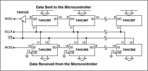
The simplest way to convert serial data (especially SPI interface data) to a parallel format is to use GPIO (general-purpose microprocessor I/O) pins. GPIOs emulate the necessary serial-port timing and add the appropriate shift register to convert the data to the correct format. For a serial-output ADC, use a serial-in/parallel-out shift register (such as the 74HC595 or equivalent) to convert the serial-conversion data to a parallel format. For a DAC, use a parallel-in/serial-out shift register (such as the 74HC597 or equivalent) to convert the parallel DAC data to a serial-output stream.
BACK TO QUESTIONS
How Can I Debug (or Probe) an SPI Interface?
When debugging an SPI interface, an SPI slave device such as Figure 1 can be useful. This circuit uses shift registers to convert data to a parallel format, which can be latched if necessary.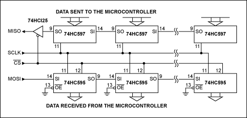
Figure 1. When driven by an SPI master, this circuit converts the SPI signals to steady outputs for easy probing.
BACK TO QUESTIONS
What Is Bit-Banging?
Bit-banging is a method of using GPIO lines to emulate a serial port. Microcontrollers with serial-port modules like SPI and I2C manage all synchronization and timing signals; the activity is transparent to the user. With bit-banging, however, each write to the port causes a single transition at the port pin. The user, first, must provide the correct number of transitions to obtain the desired waveform and, second, ensure that the timing requirements (particularly the setup and hold times for reading and writing data) are met. There is overhead associated with the number of writes to the port. Consequently, while the actual port speed might be quite high, the actual bit-bang throughput rate is usually very slow.
BACK TO QUESTIONS
My Microcontroller Has No SPI Interface. Can I Use Bit-Banging?
The following pseudo-code subroutine simultaneously reads and writes 8 bits through a synchronous serial interface. (Some microprocessors offer specialized hardware that performs this job. Examples include Motorola's 68HC11 SPI and QSPI?, and National Semiconductor's? MICROWIRE.) This outline describes a common substitute interface that is implemented by setting and clearing individual output pins.
Depending on the speed of the processor, delays may be required to satisfy the interface timing requirements.
Pin Definitions for the Pseudo-Code Subroutine
*SCK: the serial clock input to the Maxim chip
*DIN: the serial data input to the Maxim chip
*DOUT: the serial data output from the Maxim chip
Pseudo-Code Subroutine
int read_write_synchronous_serial (int write_value)
{

        read_value = 0 /* read_value will accumulate the input value */
        drive SCK pin low
        for (count = 0 to 7) /* process each of the eight bits */
        {

        read_value = read_value * 2 /* shift input value left */
        if (write_value bit 7 is 1) /* write the data, MSB first */

        then drive din pin high
        else drive din pin low

        /* delay here to satisfy data setup time and minimum clock low time */
        drive SCK pin high /* clock rising edge happens here */
        if (DOUT pin is high) /* sample the received data, LSB last */

        then read_value = read_value + 1

        /* delay here to satisfy data hold time and minimum clock high time */
        drive SCK pin low /* clock falling edge happens here */
        write_value = write_value * 2 /* shift output value left */

        }
        return read_value

}
BACK TO QUESTIONS
What Is the MICROWIRE Interface?
MICROWIRE is a serial interface standard defined by National Semiconductor. The MICROWIRE protocol is essentially a subset of the SPI interface, namely CPOL = 0 and CPHA = 0. (See "What Is the SPI Interface?" above).
BACK TO QUESTIONS
What Is the I2C Interface?
I2C is a 2-wire serial interface standard defined by NXP? Semiconductors (formerly Philips Semiconductor). The key advantage of the I2C interface is that only two lines (clock and data) are required for full-duplexed communication between multiple devices. (In contrast, SPI requires a minimum of three to four lines with a single device on the bus). The interface typically runs at a fairly low speed (100kHz to 400kHz). With I2C, each IC on the bus has a unique address. To begin communication, the bus master (typically a microcontroller) places the address of the slave device on the bus. All slave ICs monitor the bus to determine if the master device is sending a address. Only the device with the correct address communicates with the master.
Note that with other serial protocols such as SPI, a chip-select input is required to enable the IC. Thus, when 10 devices are on the bus, 10 chip-select lines plus the shared clock and data lines are needed to select the appropriate device. For I/O-constrained applications, these many lines can present quite a challenge. In contrast, I2C requires only two control lines with 10 devices on the bus.
BACK TO QUESTIONS
My Microcontroller Has No I2C Interface. Can I Use Bit-Banging?
The following code reads and writes 8 bits using a 2-wire interface. (Some microprocessors offer specialized hardware that performs this job. Examples include NXP? Semiconductors' (formerly Philips Semiconductor) 8051 family. The outline below describes a common substitute interface, implemented by setting and clearing individual output pins. This process is also known as "bit-banging."
Depending on the microcontroller's speed, delays may be required to satisfy the interface timing requirements.
Pin Definitions for the Code
* SCL: 2-wire (I2C) clock
* SDA: 2-wire (I2C) data
Code
//---------------------------------------------------------------------------
// Define the physical interface hardware.
// The __int8 type represents an 8-bit integer.
// Note: True I2C requires open-collector drivers.
// If you are using open-collector gates (such as 74HC05), inversion may be required.
// The physical interface shown here does not invert incoming or outgoing data.

// Assert SCL to a LOW level.
void AssertSCL(void) { Write_Pin(1,0); }

// Release SCL to be pulled to a HIGH level.
void ReleaseSCL(void) { Write_Pin(1,1); }

// Get the SCL level: Return 0 if SCL is LOW, return 1 if SCL is HIGH.
int GetSCL (void) { return Read_Pin(1); }

// Assert SDA to a LOW level.
void AssertSDA(void) { Write_Pin(2,0); }

// Release SDA to be pulled to a HIGH level.
void ReleaseSDA(void) { Write_Pin(2,1); }

// Get the SDA level: Return 0 if SCL is LOW, return 1 if SCL is HIGH.
int GetSDA (void) { return Read_Pin(2); }

//---------------------------------------------------------------------------
// Make sure that the clock actually goes high.
// Some other slave device may be stretching the clock.
bool Make_Sure_SCL_is_High(void)
{

        if (GetSCL() != 0)

        return true;    // Success: Clock is high.

        while (GetSCL() != 1)
        {

        // Wait until clock goes high.
        // A practical implementation should include a timeout handler.

        }
        return true;    // Success

}

//---------------------------------------------------------------------------
// TwoWireMasterStart:
// Send a start condition on the bus.
bool TwoWireMasterStart(void)
{

        ReleaseSDA();
        ReleaseSCL();
        Delay40usec();
        Make_Sure_SCL_is_High();
        AssertSDA();
        Delay47usec();
        AssertSCL();
        return true;

}

//---------------------------------------------------------------------------
// TwoWireMasterStop:
// Send a stop condition, releasing the bus.
bool TwoWireMasterStop(void)
{

        AssertSCL();
        AssertSDA();
        Delay47usec();  // Minimum clock low time
        ReleaseSCL();
        Delay40usec();
        Make_Sure_SCL_is_High();
        ReleaseSDA();
        Delay47usec();
        return true;

//---------------------------------------------------------------------------
// TwoWireMasterWrite:
// Transmit 8 bits on the SM bus, and check for an acknowledge.
//
// On Entry:
//      Byte = the 8 bit value to transmit
//      A start condition must have been previously established.
//
// On Exit:
//      Return value = 0 if the byte was not acknowledged (NACK)
//      Return value = 1 if the byte was acknowledged (ACK)
bool TwoWireMasterWrite(const __int8 byte)
{

        __int8 temp = byte;
        for (int i = 1; i <= 8; i = i + 1)
        {

        AssertSCL();
        if (temp & 0x80)
                ReleaseSDA();
        else
                AssertSDA();
        temp = temp + temp;    // shift left
        Delay47usec();
        ReleaseSCL();
        Delay40usec();
        Make_Sure_SCL_is_High();

}

//---------------------------------------------------------------------------
// RxSMBusByte:
//
// Read 8 bits from the SM bus.
// ACK / NACK is handled separately by RxSMBusByteACK / RxSMBusByteNACK.
// This function is called by both TwoWireMasterReadContinued and TwoWireMasterReadLast.
//
// On Entry:
//    A start condition must have been previously established,
//    and a slave must have been addressed in master read mode.
//
// On Exit:
//    Return value = byte read from the bus
__int8 RxSMBusByte (void)
{

        __int8 byte = 0;
        ReleaseSDA();
        for (int i = 1; i <= 8; i = i + 1)
        {

        AssertSCL();    // Pull SCL low so that data can change.
        Delay47usec();  // Allow SDA time to change.
        ReleaseSCL();   // Clock edge
        Delay40usec();  // SDA should be steady while SCL is high.
        Make_Sure_SCL_is_High();
        byte = byte + byte;     // MSB first, LSB last.
        if (GetSDA())
                byte = byte + 1;        // Set the LSB.

        {
        return byte;

{

//---------------------------------------------------------------------------
// Call this function to read a byte, when you plan to read some more bytes.
__int8 TwoWireMasterReadContinued(void)
{

        __int8 data = RxSMBusByte();
        AssertSCL();    // Pull SCL low so that data can change.
        AssertSDA();    // Send ACK to slave.
        Delay47usec();  // Setup time
        ReleaseSCL();   // Clock the ACK pulse into the slave.
        Delay47usec();  // Hold time
        Make_Sure_SCL_is_High();
        AssertSCL();
        return data;

{

//---------------------------------------------------------------------------
// Call this function to read the last byte of data.
__int8 TwoWireMasterReadLast(void)
{

        __int8 data = RxSMBusByte();
        AssertSCL();    // Pull SCL low so that data can change.
        ReleaseSDA();   // Send NACK to slave.
        Delay47usec();  // Setup time
        ReleaseSCL();   // Clock the ACK pulse into the slave.
        Delay47usec();  // Hold time
        Make_Sure_SCL_is_High();
        AssertSCL();
        return data;

{
BACK TO QUESTIONS
PCB Layout Guidelines
This section includes PCB layout guidelines and discusses prototyping issues.
Do You Have Any General Circuit-Layout Tips?
In the application note 637, "Tech Tips: Getting the Most from Your Sensor and Conditioning Electronics," you will find tips for good PCB layout. Though this article is targeted for PRT (piezoresistive transducer) designs, the principles are general enough so that they are applicable to other circuits as well. Maxim has many other PCB application notes that can help you.
BACK TO QUESTIONS
Do You Have Any Circuit-Layout Tips for ADCs?
Partition the system into analog, digital, and power-supply sections. Group the related components together. Draw a physical boundary between the analog and digital sections. The ADC should straddle the boundary between analog and digital. Nothing else should cross this boundary, except the ADC and a single, carefully selected power and ground return.
Digital traces should never cross analog traces; they should not even pass over an analog ground. Digital traces should be routed away from sensitive analog traces. When digital traces are near analog traces, even though there is no direct connection, the PCB's parasitic capacitance will couple high-frequency noise from any nearby switching signals into the analog signal. The faster the signal switches, the more it will interfere with analog signals. The proper handling of analog-versus-digital ground connections can have a significant impact on the overall system performance. For grounding issues, see "Do You Have Any Grounding/Ground Plane Tips?" below.
BACK TO QUESTIONS
Do You Have Any Grounding/Ground Plane Tips?
A ground plane is recommended, especially for high-resolution or high-frequency applications. However, deciding to use a ground plane depends mainly on your intent. If, for example, you only want to determine the basic functionality of an IC, a simple proto-board may be adequate. If you are observing AC performance, expect the proto-board to provide less-than-optimal performance, and as frequency increases the performance can degrade drastically.
A ground plane is simply an area of a PCB (an entire layer or a portion of it) that provides a low-impedance return path for current flow. As current flows, any resistance encountered will appear as an IR (voltage) drop. Thus, if the ground plane has an appreciable resistance, the associated IR voltage drop will result in variations in the ground-plane potential. This, in turn, can have very adverse consequences, such as localized ground-current loops and excessive current flow due to the mismatch in ground potentials.
Sensitive analog circuitry requires a quiet ground plane. In some cases, a circuit board may consist of separate analog and digital power-supply planes and separate analog and digital ground planes to isolate the digital noise from the analog circuitry. Other applications use a single supply, but partition the board as if separate analog and digital supplies were used. In the latter case, chokes, ferrite beads, and adequate bypassing provide a "clean" analog supply that is treated as separate from the digital supply.
The analog and digital ground planes reside on the same physical PCB layer, but are set up so that the currents from the digital circuitry do not interact with the currents from the analog circuitry. This is done by physically separating analog and digital components and providing an imaginary division on the board. This division ensures that the digital currents flow on the "digital" side and the analog currents flow on the "analog" side.
Mixed-signal components that are both analog and digital straddle the analog and digital ground planes. With these ICs, connect their analog and digital ground pins together at the chip by using very short traces. Connect this to a single point at the intersection of the analog and digital ground planes.
Digital signals such as those from microprocessors, ASICs, DSPs, and digital logic are very noisy due to the large transient current spikes as the logic levels change. In addition, switching power supplies, machinery (e.g., motors or actuators), and EMI are potential sources of noise that can couple into sensitive analog circuitry.
The key to a successful design is to decouple (or isolate) the sensitive analog circuitry from these noise sources. In simple terms, keep the digital noise confined to the digital ground plane. Because the digital ground current is comprised of a series of current spikes, chokes and inductors are used to filter these spikes and prevent them from coupling to the analog circuitry.
You can minimize noise by following these suggestions:
- Connect analog and digital ground pins together at a single point near the IC.
- Connect the analog and digital ground planes together at a single point by using a star ground connection.
- Keep signal and ground traces short. Long traces have more inductance and higher resistance.
- Do not route digital lines (especially clocks) near the analog ground plane.
- Use linear regulators instead of switching regulators.
- Provide a shield around sensitive analog circuits by placing a "ring" around the analog components. Connect this ring to analog ground.
- Separate parallel traces to minimize capacitive coupling.
- Do not run analog and digital traces parallel to each other, as there is inductive coupling between parallel traces.
BACK TO QUESTIONS
Can the 0.1μF Bypass Capacitors Be Eliminated?
The system will not function correctly without proper bypass capacitors. Bypass capacitors are required, because whenever the IC switches, it generates a transient current load on the power-supply and ground-return traces. In accordance with Ohm's law, the power-supply voltage to the chip drops, and the IC's ground pin is raised above the system ground due to these transient current effects. The transients are exacerbated by the typical series inductance of the power-supply traces, which cause magnetically induced voltages to oppose the change in current flow. This is a problem both when the current begins spiking up, and when it tries to return to its initial level.
A bypass capacitor located physically close to the IC solves this problem by canceling some of the power-supply lead inductance. Of course, the energy still has to flow from the power supply to the IC, but the bypass capacitor provides a small reservoir of energy to quickly satisfy the local surge without causing significant overshoot or droop at the IC's power-supply pins.
As a general rule, each IC should have a direct connection to a 0.1μF ceramic capacitor located no more than about 5mm away. This forms a loop where transient switching currents for that IC circulate. Do not mix unrelated loops. The route is from the IC, to the capacitor, to the power-supply busses.
In addition to the small ceramic capacitors, there should be some larger bulk capacitors located where the power-supply connections enter the PCB assembly. The capacitor value should be between 10μF and 1000μF, depending on the system's needs. Remember to consider the voltage ratings. If the power supply is 5V, use at least a 10V-rated capacitor or even higher if the system is exposed to high temperature.
BACK TO QUESTIONS
How Can I Model the Real-World Effects of PCBs?
A PCB adds some capacitance, resistance, and inductance to the circuit. These parasitic circuit elements can change with temperature, mechanical stress, and even age. If you are a fan of SPICE models, you can always add these parasitic elements to the circuit to check for sensitivity. But it is impossible to develop a rigorous model without verifying physical performance. You need to build a prototype.
Consider a typical four-layer FR4 dielectric PCB with 1-ounce copper plating and a net thickness of 0.0625in. The thickness of 1-ounce copper plating is 0.00139in. The distance between layers is 0.019in.
You can estimate the resistance of a PCB trace based on its shape. Tile the trace with squares, and then multiply the foil sheet resistance by the number of squares. Standard 1-ounce copper foil has a thickness of 0.00139in, which corresponds to a sheet resistance of 0.49mΩ per square. (This resistance varies ±25% over -40°C to +85°C.) So, a PCB trace that is 0.010in wide and 1.000in long has a resistance of 100 squares, or approximately 0.05Ω. If a switching transient of 500mA flowed through this trace (even for a microsecond), the voltage drop across it would be 25mV.
There is parasitic capacitance between adjacent traces on the same layer and between traces on adjacent layers as well. The common FR4 material has a relative dielectric between 4 and 5, although it is not usually controlled tightly. Often the parasitic capacitance is a few picofarads, but it can be higher if the board is dirty.
BACK TO QUESTIONS
Debugging and Diagnostics
This section deals with diagnostic techniques that can help during the prototype stage.
Why Am I Not Getting the Specified Accuracy from My ADC?
There are several potential sources of error, including the power supplies, open circuits, short circuits, poor layout, malfunctioning external components, and the actual device itself.
The quickest way to resolve the problem is to obtain an EV (evaluation) kit for the device. Maxim provides many ADC EV kits with user-friendly software. A kit will allow you to quickly exercise the IC and analyze its performance.
If using an EV kit is not an option, first check your board for shorts and open circuits. Next, check the voltages on each pin of the IC. Use an oscilloscope rather than a DMM so that any noise or oscillations will be observed. Try a different component in the socket. Finally, check the external components; "bad" capacitors and resistors can cause circuit anomalies.
If the problem still persists, refer to application note 748, "The ABCs of ADCs: Understanding How ADC Errors Affect System Performance," to determine if the ADC's performance could be the culprit.
BACK TO QUESTIONS
Why Is the Output Code Stuck at All Ones?
This could happen if the voltage reference is not working properly. Check the reference voltage. Perhaps the reference input was inadvertently shorted to ground. Use a handheld DVM to measure between the reference input and ground, right at the ADC's pins.
If the ADC has a shutdown pin, use an oscilloscope to verify that shutdown is not active. Some parts permit the shutdown pin to be left unconnected (floating); other parts require it to be driven high or low.
Use an oscilloscope to check the DOUT pin of the ADC. See if the part is performing conversions. Perhaps there is a wire broken somewhere.
BACK TO QUESTIONS
Why Are the ADC Measurements Noisy?
Finding the source of noise in ADC measurements is not always easy. The following suggestions will help you arrive at the source of the problem quickly.
- Check the test hardware to make sure that the test setup is not the source of the problem.
- Are the power supplies clean? Do they have adequate bypassing at the ADC power-supply pins?
- Has the circuit board been checked for shorts, proper pin configurations, short traces, an adequate low-noise ground, etc.?
- Is the reference voltage at the correct value? If an external reference is used, does it have low enough noise? Can it source adequate current?
- Is the circuit being tested in a relatively noise-free environment? If not, move to one. Noise tends to find its way into circuits through the power supplies, EMI (electromagnetic interference), lighting, and a host of other sources.
- Determine if the noise could be coming from the input-signal source, the analog front-end signal conditioning circuitry, or the ADC itself. Observe the signal source on a spectrum analyzer or an oscilloscope, and examine the output of the front-end circuitry in a similar manner. If an op amp is used on the front-end, make sure that its noise performance is acceptable for the performance desired.
- In addition, verify that the ADC has adequate bandwidth at the frequencies of interest. Other things to check are the scope probes, the power supplies for excessive current flow, and the ADC's programmed state to make sure that the correct programming information was written to the ADC. Is the oscilloscope floating or is it powered by 50Hz/60Hz? This could have affect the noise performance. There also could be other signals getting into the ADC input. Is there a lowpass filter on the ADC input to remove high-frequency noise?
Keep in mind that a logical, systematic approach will lead to the source of the noise much faster than a trial-and-error method.
BACK TO QUESTIONS
I Noticed Noise from the MAX194/MAX195. How Do I Get Rid of It?
The MAX194/MAX195's LSB (least-significant bit) size is slightly less than the RMS code-edge noise level. This means that the peak-to-peak noise is greater than an LSB. Thus, the LSB is actually in the noise of the converter. However, averaging can effectively reduce this noise. "N" samples will reduce the noise by a factor of the square root of N. For improved noise performance, consider using the MAX1132 for new designs.
 電子發(fā)燒友App





評論