This application note answers general frequently asked questions (FAQs) about analog switches. The FAQs also cover topics specific to Maxim switches.
This set of frequently asked questions (FAQs) addresses some of the more common issues that arise when using Maxim broadband analog switches in new or existing designs. The questions are divided into different catmaxegories based on specific information areas. It is possible for questions to span multiple categories.
Also see
A1. Most engineers understand that a bandwidth of 650MHz is more than enough to pass 10BASE-T (10Mbps) as well as 100BASE-T (100Mbps, Fast Ethernet) signals. It is, however, not so obvious to many that this bandwidth is sufficient for 1000BASE-T (1Gbps, Gigabit Ethernet). This misunderstanding probably stems from the prevalence today of two-level non-return-to-zero (NRZ) transmission schemes.
In Gigabit Ethernet, the data payload is split across all four of the twisted pairs of the Ethernet cabling, 250Mbps per pair. The transition rate is further reduced, using a five-level pulse amplitude modulation (PAM-5) scheme that trades multiple amplitude levels for baud rate. The result is that 1000BASE-T transmits data at 125 million transitions per second, the same as Fast Ethernet. Therefore, any cabling system with analog bandwidth sufficient to convey Fast Ethernet should also be able to convey Gigabit Ethernet.
For LAN switches such as the MAX4890, a bandwidth of 650MHz is more than adequate.
Q2. I cannot switch 625Mbps LVDS signals with the MAX4890, yet it apparently passes 1Gbps Ethernet. Why is that? Please explain.
A2. Because of the coding method used, Gigabit Ethernet only transmits at 125 million transitions per second per pair. To achieve similar performance, LVDS would need to transmit at 125Mbps per pair. Because of Gigabit Ethernet's multiple pulse amplitude coding scheme (PAM-5), it transmits 2 bits per transition versus the LVDS 1 bit per transition.
Q3. The MAX4890 does not appear to transmit Ethernet signals properly and the signals coming out appear to be severely clipped. How can I fix this?
A3. The MAX4890 needs the Ethernet signals that it switches to be between V+ (around 3.3V) and ground. Any signal excursions beyond these limits will get clipped by the ESD clamps on those pins. This is usually not an issue because most PHYs drive their Ethernet interfaces between V+ and ground. However, this is not universal practice. Some PHYs provide a ±1V excursion around 3.3V!
If the Ethernet signal to be switched passes beyond these limits, the board designer must rebias these signals to an appropriate range. Ethernet signals can be effectively DC blocked with series capacitors. Also, center-tapped transformers make it straightforward to rebias to almost any desired DC point.
Q4. How can I evaluate or prototype the MAX4890 into my design before including it in my circuit?
A4. Contact your Maxim Account Manager, FAE, or contact customer support. Ask for the MAX4890 LAN prototype evaluation (EV) board.
This EV board requires some care when it is attached to your circuit. The schematic is shown: here.
A1. No. The MAX4888 consists of four isolated SPDT electronic switches, and the MAX4889 consists of eight isolated SPDT electronic switches, each of which can be a signal independent of all the others. The MAX4889 will just as easily switch eight single-ended signals as it does four differential pairs.
Q2. What Maxim product can I use to switch SGMII?
A2. The MAX4888 series of devices powered from a 3.3V supply would be ideal. SGMII switches 1.25Gbps with a VIH (max) of 1.525V, well within the capabilities of the MAX4888 products.
Q3. What Maxim product can I use to switch XAUI signals?
A3. Depending on the DC bias of the XAUI signals being switched, either the MAX4889B or the MAX4889C would be ideal. Please contact your local Account Manager and/or FAE for further support.
Q4. I need to simulate an application that includes the MAX4889B and MAX4889C. What can Maxim provide to help with this?
A4. The following 4-Port S-Parameters are between each given differential pair.
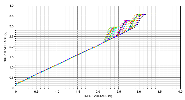
A5. Yes. The MAX4889 will drive its outputs up to about 2.2V in the worst case. After that, for a higher voltage the pass switches eventually go to high resistance. By attaching a 1kΩ pullup, you can use the MAX4889 to switch between a high-speed signal and low-speed logic. The data rate for the low-speed logic will be limited by the RC of the pullup.
A graphic detailing the input-output relationship through a given switch can be found below.
Q6. What requirements are there for using the MAX4950 in a PCIe hot-plug application?
A6. If a card is removed and the MAX4950 has not detected a load, it times out and stops checking. If a card is plugged in after this point, you will need to toggle either the Rx detect pin or the enable pin. This action will cause the MAX4950 to recheck for the termination resistance which indicates that a card is present.
Q7. Why does Maxim not provide an IBIS model of the MAX4950?
A7. Today IBIS models are ill suited to handle equalization. Suitable S-parameters are shown here. Please contact your local Maxim sales representative for alternatives.

Q8. I need to switch two XAUI interfaces. What Maxim silicon would help me do this?
A8. The MAX4889C would be ideal for this application. It can switch one of two XAUI interfaces to a third one.
Q9. I need to switch some LVDS interfaces. Can I use the MAX4889A?
A9. Yes. Both the MAX4888A and the MAX4889A can do this, but you must be sure to use a 3.3V supply. The MAX4892E can be used as well.
A1. Care must be taken when performing these measurements. Typically, the only reasonable access to the MAX4951/MAX4951A/MAX4951B/MAX4951AE is from a SATA connector at the edge of a PCB. We describe the technique used to get reproducible measurements found here.
Q2. Can Maxim provide layout guidelines for the MAX4951/MAX4951A/MAX4951B/MAX4851AE?
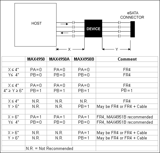
A2. Yes. Layout guidelines are shown below.
Q3. When performing SATA compliance measurements with the MAX4951/MAX4951A/MAX4591B/MAX4851AE, I get a marginal eye, especially against the top of the inner eye mask. I expected more margin here.
A3. Care must be taken when performing these measurements. We found that the front-end bandwidth of the scope used for compliance measurements makes a significant difference for eye margin. A comparison of eye openings versus oscilloscope bandwidth can be found here.
Q4. Are there any general guidelines for where to position the MAX4951/MAX4951A/MAX4951B/MAX4851AE in a system?
A4. As a general guideline, the best location for the MAX4951/MAX4951A/MAX4951B/MAX4951AE is near the SATA connector itself. Depending on the trace lengths to the SATA source, you can optionally set the boost. Please contact the factory with any questions regarding layout and placement of the MAX4951/MAX4951A/MAX4951B/MAX4951AE.
Q5. I need to simulate a MAX4951/MAX4951A/MAX4951B/MAX4851AE in my application. Can Maxim provide a model for this device?
A5. Yes, Maxim can! A functional SPICE model can be found here, and an IBIS model can be found here.
Q6. When I plug in an eSATA drive before powering up the PC, the drive is recognized. However, if I plug it in after the PC is powered up, the drive is not recognized? How can I solve this?
A6. This is not a MAX4951/MAX4951A/MAX4951B/MAX4951AE issue, but a driver issue. SATA and eSATA support hot-plugging hard disk drives (HDDs) like USB drives, but this requires AHCI to be enabled by the BIOS and AHCI drivers to be installed by the operating system.
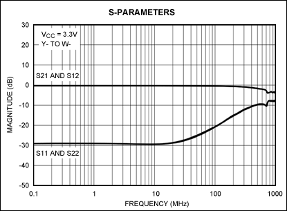
A1. An S-parameter model for a MAX4989 switch is shown here.
A1. We sure can! You can find a document detailing this application here.
Q2. Can the MAX4888 be used to switch VGA RGB signals?
A2. Yes, this is not a problem. VGA RGB signals can go up to about 0.7V, so you need to keep the MAX4888 VCC above 1.9V. The MAX4888 more than adequate bandwidth for this application.
Q3. Roughly what Bill of Materials (BOM) content does the MAX4895E replace?
A3. The MAX4895E provides ESD protection and level translation. This integration typically replaces seven diodes, two FETs, and two buffer ICs with the one, tiny 3mm x 3mm package.
Q4. The MAX4885 IBIS model will not compile in Altium when I try to simulate. Why is that?
A4. This is a known issue with Altium Designer? software. The work-around depends on whether the MAX4885 is used as a 1:2 or 2:1 multiplexer.
If M = 0, this is 1:2 mode and the buffers are enabled. Change the PIN MAPPING section by deleting the two lines that begin with "5" and the two lines that begin with "6." This will remove the switching functionality of the MAX4885 for the H and V outputs, but still permits simulation for other purposes such as signal integrity.
If M = 1, this is 2:1 mode and the buffers are disabled. Change the PIN section so that the models for pins 18, 19, 22, and 23 change from HVMUXOUT to TERM1.
Q5. I would like to use the MAX4895E in an application where the SDA1 and SCL1 lines can be powered from a monitor plugged into a VGA connector while the MAX4895E itself is not powered. Will this work?
A5. This will work, as long as you isolate the MAX4895E’s VCC pin with a diode to prevent reverse current flow.
A1. Yes it does. The MAX4820 has an internal 8-bit shift register to collect serial data. If you have performed a write operation by asserting active-low CS low, clocked in 8 bits of data, and then deasserted active-low CS high, that data remains in the MAX4820's shift register
During a second write operation DOUT will clock out the 8 bits of the previous write operation.
Example sequence: (X7-0 and Y7-0 are arbitrary bits)
Active-low CS low
SCLK rising, DIN = X7
SCLK falling, DOUT = ?
SCLK rising, DIN = X6
SCLK falling, DOUT = ?
SCLK rising, DIN = X5
SCLK falling, DOUT = ?
SCLK rising, DIN = X4
SCLK falling, DOUT = ?
SCLK rising, DIN = X3
SCLK falling, DOUT = ?
SCLK rising, DIN = X2
SCLK falling, DOUT = ?
SCLK rising, DIN = X1
SCLK falling, DOUT = ?
SCLK rising, DIN = X0
SCLK falling, DOUT = ?
Active-low CS high
{wait a bit}
Active-low CS low
SCLK risin, DIN = Y7
SCLK falling, DOUT = X7
SCLK rising, DIN = Y6
SCLK falling, DOUT = X6
SCLK rising, DIN = Y5
SCLK falling, DOUT = X5
SCLK rising, DIN = Y4
SCLK falling, DOUT = X4
SCLK rising, DIN = Y3
SCLK falling, DOUT = X3
SCLK rising, DIN = Y2
SCLK falling, DOUT = X2
SCLK rising, DIN = Y1
SCLK falling, DOUT = X1
SCLK rising, DIN = Y0
SCLK falling, DOUT = X0
Active-low CS high
In this example, the active-low CS, SCLK, and DIN signals control the MAX4820; DOUT is driven by the MAX4820.
Altium Designer is a registered trademark of Altium Limited.
Altium is a registered trademark of Altium Limited.
PCI Express is a registered trademark of PCI-SIG Corp.
PCIe is a registered trademark of PCI-SIG Corp.
This set of frequently asked questions (FAQs) addresses some of the more common issues that arise when using Maxim broadband analog switches in new or existing designs. The questions are divided into different catmaxegories based on specific information areas. It is possible for questions to span multiple categories.
Also see
- Application note 638, "Selecting the right CMOS analog switch."
- Application note 4714, "Webinar: Specification and selection of analog switches and multiplexers"
LAN questions
- How does the MAX4890 pass Ethernet signals, including Gigabit Ethernet, when it has a bandwidth of only 650MHz?
- I cannot switch 625Mbps LVDS signals with the MAX4890, yet it apparently passes 1Gbps Ethernet. Why is that? Please explain.
- The MAX4890 does not appear to transmit Ethernet signals properly and the signals coming out appear to be severely clipped. How can I fix this?
- How can I evaluate or prototype the MAX4890 into my design before including it in my circuit?
PCI Express? questions
- For each pair of pins switched on the MAX4888/MAX4889 devices, for example, NC1+ and NC1-, must they switch a differential pair?
- What Maxim product can I use to switch SGMII?
- What Maxim product can I use to switch XAUI signals?
- I need to simulate an application that includes the MAX4889B and MAX4889C. What can Maxim provide to help with this?
- Is it possible to switch completely different types of signals like SATA or LVCMOS with the MAX4889?
- What requirements are there for using the MAX4950 in a PCIe? hot-plug application?
- Why does Maxim not provide an IBIS model of the MAX4950?
- I need to switch two XAUI interfaces. What Maxim silicon would help me do this?
- I need to switch some LVDS interfaces. Can I use the MAX4889A?
SAS/SATA questions
- How does Maxim measure SATA eyes with a MAX4951/MAX4951A/MAX4951B in a system?
- Can Maxim provide layout guidelines for the MAX4951/MAX4951A/MAX4951B?
- When performing SATA compliance measurements with the MAX4951/MAX4951A/MAX4951B, I get a marginal eye, especially against the top of the inner eye mask. I expected more margin here.
- Are there any general guidelines for where to position the MAX4951/MAX4951A/MAX4951B in a system?
- I need to simulate a MAX4951/MAX4951A/MAX4951B in my application. Can Maxim provide a model for this device?
- When I plug in an eSATA drive before powering up the PC, the drive is recognized. However, if I plug it in after the PC is powered up, the drive is not recognized? How can I solve this?
USB questions
- I need to simulate an application with the MAX4989. What can Maxim provide to help with this?
Video questions
- Can Maxim provide guidelines for using the MAX4885E in an 8:1 VGA switch application?
- Can the MAX4888 be used to switch VGA RGB signals?
- Roughly what Bill of Materials (BOM) content does the MAX4895E replace?
- The MAX4885 IBIS model refuses to compile in Altium? when I try to simulate. Why is that?
- I would like to use the MAX4895E in an application where the SDA1 and SCL1 lines can be powered from a monitor plugged into a VGA connector while the MAX4895E itself is not powered. Will this work?
Miscellaneous device questions
- On the digital serial interface of the MAX4820 relay driver, when data is shifted into the device on DIN, does the data out of the part (DOUT) represent the previous data written to the device, even across write cycles? (/CS going high, then low separates write cycles)
LAN questions
Q1. How does the MAX4890 pass Ethernet signals, including Gigabit Ethernet, when it has a bandwidth of only 650MHz?A1. Most engineers understand that a bandwidth of 650MHz is more than enough to pass 10BASE-T (10Mbps) as well as 100BASE-T (100Mbps, Fast Ethernet) signals. It is, however, not so obvious to many that this bandwidth is sufficient for 1000BASE-T (1Gbps, Gigabit Ethernet). This misunderstanding probably stems from the prevalence today of two-level non-return-to-zero (NRZ) transmission schemes.
In Gigabit Ethernet, the data payload is split across all four of the twisted pairs of the Ethernet cabling, 250Mbps per pair. The transition rate is further reduced, using a five-level pulse amplitude modulation (PAM-5) scheme that trades multiple amplitude levels for baud rate. The result is that 1000BASE-T transmits data at 125 million transitions per second, the same as Fast Ethernet. Therefore, any cabling system with analog bandwidth sufficient to convey Fast Ethernet should also be able to convey Gigabit Ethernet.
For LAN switches such as the MAX4890, a bandwidth of 650MHz is more than adequate.
Q2. I cannot switch 625Mbps LVDS signals with the MAX4890, yet it apparently passes 1Gbps Ethernet. Why is that? Please explain.
A2. Because of the coding method used, Gigabit Ethernet only transmits at 125 million transitions per second per pair. To achieve similar performance, LVDS would need to transmit at 125Mbps per pair. Because of Gigabit Ethernet's multiple pulse amplitude coding scheme (PAM-5), it transmits 2 bits per transition versus the LVDS 1 bit per transition.
Q3. The MAX4890 does not appear to transmit Ethernet signals properly and the signals coming out appear to be severely clipped. How can I fix this?
A3. The MAX4890 needs the Ethernet signals that it switches to be between V+ (around 3.3V) and ground. Any signal excursions beyond these limits will get clipped by the ESD clamps on those pins. This is usually not an issue because most PHYs drive their Ethernet interfaces between V+ and ground. However, this is not universal practice. Some PHYs provide a ±1V excursion around 3.3V!
If the Ethernet signal to be switched passes beyond these limits, the board designer must rebias these signals to an appropriate range. Ethernet signals can be effectively DC blocked with series capacitors. Also, center-tapped transformers make it straightforward to rebias to almost any desired DC point.
Q4. How can I evaluate or prototype the MAX4890 into my design before including it in my circuit?
A4. Contact your Maxim Account Manager, FAE, or contact customer support. Ask for the MAX4890 LAN prototype evaluation (EV) board.
This EV board requires some care when it is attached to your circuit. The schematic is shown: here.
PCI Express questions
Q1. For each pair of pins switched on the MAX4888/MAX4889 devices, for example, NC1+ and NC1-, must they switch a differential pair?A1. No. The MAX4888 consists of four isolated SPDT electronic switches, and the MAX4889 consists of eight isolated SPDT electronic switches, each of which can be a signal independent of all the others. The MAX4889 will just as easily switch eight single-ended signals as it does four differential pairs.
Q2. What Maxim product can I use to switch SGMII?
A2. The MAX4888 series of devices powered from a 3.3V supply would be ideal. SGMII switches 1.25Gbps with a VIH (max) of 1.525V, well within the capabilities of the MAX4888 products.
Q3. What Maxim product can I use to switch XAUI signals?
A3. Depending on the DC bias of the XAUI signals being switched, either the MAX4889B or the MAX4889C would be ideal. Please contact your local Account Manager and/or FAE for further support.
Q4. I need to simulate an application that includes the MAX4889B and MAX4889C. What can Maxim provide to help with this?
A4. The following 4-Port S-Parameters are between each given differential pair.
- 4-Port S-Parameter Plots, Differential and Common Mode
- 4-Port S-Parameter Plots, Single Ended Graphs
- 4-Port S-Parameters, in Touchstone format
A5. Yes. The MAX4889 will drive its outputs up to about 2.2V in the worst case. After that, for a higher voltage the pass switches eventually go to high resistance. By attaching a 1kΩ pullup, you can use the MAX4889 to switch between a high-speed signal and low-speed logic. The data rate for the low-speed logic will be limited by the RC of the pullup.
A graphic detailing the input-output relationship through a given switch can be found below.

Q6. What requirements are there for using the MAX4950 in a PCIe hot-plug application?
A6. If a card is removed and the MAX4950 has not detected a load, it times out and stops checking. If a card is plugged in after this point, you will need to toggle either the Rx detect pin or the enable pin. This action will cause the MAX4950 to recheck for the termination resistance which indicates that a card is present.
Q7. Why does Maxim not provide an IBIS model of the MAX4950?
A7. Today IBIS models are ill suited to handle equalization. Suitable S-parameters are shown here. Please contact your local Maxim sales representative for alternatives.

Q8. I need to switch two XAUI interfaces. What Maxim silicon would help me do this?
A8. The MAX4889C would be ideal for this application. It can switch one of two XAUI interfaces to a third one.
Q9. I need to switch some LVDS interfaces. Can I use the MAX4889A?
A9. Yes. Both the MAX4888A and the MAX4889A can do this, but you must be sure to use a 3.3V supply. The MAX4892E can be used as well.
SAS/SATA questions
Q1. How does Maxim measure SATA eyes with a MAX4951/MAX4951A/MAX4951B and MAX4951AE in a system?A1. Care must be taken when performing these measurements. Typically, the only reasonable access to the MAX4951/MAX4951A/MAX4951B/MAX4951AE is from a SATA connector at the edge of a PCB. We describe the technique used to get reproducible measurements found here.
Q2. Can Maxim provide layout guidelines for the MAX4951/MAX4951A/MAX4951B/MAX4851AE?
A2. Yes. Layout guidelines are shown below.

Q3. When performing SATA compliance measurements with the MAX4951/MAX4951A/MAX4591B/MAX4851AE, I get a marginal eye, especially against the top of the inner eye mask. I expected more margin here.
A3. Care must be taken when performing these measurements. We found that the front-end bandwidth of the scope used for compliance measurements makes a significant difference for eye margin. A comparison of eye openings versus oscilloscope bandwidth can be found here.
Q4. Are there any general guidelines for where to position the MAX4951/MAX4951A/MAX4951B/MAX4851AE in a system?
A4. As a general guideline, the best location for the MAX4951/MAX4951A/MAX4951B/MAX4951AE is near the SATA connector itself. Depending on the trace lengths to the SATA source, you can optionally set the boost. Please contact the factory with any questions regarding layout and placement of the MAX4951/MAX4951A/MAX4951B/MAX4951AE.
Q5. I need to simulate a MAX4951/MAX4951A/MAX4951B/MAX4851AE in my application. Can Maxim provide a model for this device?
A5. Yes, Maxim can! A functional SPICE model can be found here, and an IBIS model can be found here.
Q6. When I plug in an eSATA drive before powering up the PC, the drive is recognized. However, if I plug it in after the PC is powered up, the drive is not recognized? How can I solve this?
A6. This is not a MAX4951/MAX4951A/MAX4951B/MAX4951AE issue, but a driver issue. SATA and eSATA support hot-plugging hard disk drives (HDDs) like USB drives, but this requires AHCI to be enabled by the BIOS and AHCI drivers to be installed by the operating system.
USB questions
Q1. I need to simulate an application with the MAX4989. What can Maxim provide to help with this?A1. An S-parameter model for a MAX4989 switch is shown here.

Video questions
Q1. Can Maxim provide guidelines for using the MAX4885E in an 8:1 VGA switch application?A1. We sure can! You can find a document detailing this application here.
Q2. Can the MAX4888 be used to switch VGA RGB signals?
A2. Yes, this is not a problem. VGA RGB signals can go up to about 0.7V, so you need to keep the MAX4888 VCC above 1.9V. The MAX4888 more than adequate bandwidth for this application.
Q3. Roughly what Bill of Materials (BOM) content does the MAX4895E replace?
A3. The MAX4895E provides ESD protection and level translation. This integration typically replaces seven diodes, two FETs, and two buffer ICs with the one, tiny 3mm x 3mm package.
Q4. The MAX4885 IBIS model will not compile in Altium when I try to simulate. Why is that?
A4. This is a known issue with Altium Designer? software. The work-around depends on whether the MAX4885 is used as a 1:2 or 2:1 multiplexer.
If M = 0, this is 1:2 mode and the buffers are enabled. Change the PIN MAPPING section by deleting the two lines that begin with "5" and the two lines that begin with "6." This will remove the switching functionality of the MAX4885 for the H and V outputs, but still permits simulation for other purposes such as signal integrity.
If M = 1, this is 2:1 mode and the buffers are disabled. Change the PIN section so that the models for pins 18, 19, 22, and 23 change from HVMUXOUT to TERM1.
Q5. I would like to use the MAX4895E in an application where the SDA1 and SCL1 lines can be powered from a monitor plugged into a VGA connector while the MAX4895E itself is not powered. Will this work?
A5. This will work, as long as you isolate the MAX4895E’s VCC pin with a diode to prevent reverse current flow.
Miscellaneous device questions
Q1. On the digital serial interface of the MAX4820 relay driver, when data is shifted into the device on DIN, does the data out (DOUT) represent the previous data written to the device, even across write cycles (i.e., active-low CS going high, then low separates write cycles)?A1. Yes it does. The MAX4820 has an internal 8-bit shift register to collect serial data. If you have performed a write operation by asserting active-low CS low, clocked in 8 bits of data, and then deasserted active-low CS high, that data remains in the MAX4820's shift register
During a second write operation DOUT will clock out the 8 bits of the previous write operation.
Example sequence: (X7-0 and Y7-0 are arbitrary bits)
Active-low CS low
SCLK rising, DIN = X7
SCLK falling, DOUT = ?
SCLK rising, DIN = X6
SCLK falling, DOUT = ?
SCLK rising, DIN = X5
SCLK falling, DOUT = ?
SCLK rising, DIN = X4
SCLK falling, DOUT = ?
SCLK rising, DIN = X3
SCLK falling, DOUT = ?
SCLK rising, DIN = X2
SCLK falling, DOUT = ?
SCLK rising, DIN = X1
SCLK falling, DOUT = ?
SCLK rising, DIN = X0
SCLK falling, DOUT = ?
Active-low CS high
{wait a bit}
Active-low CS low
SCLK risin, DIN = Y7
SCLK falling, DOUT = X7
SCLK rising, DIN = Y6
SCLK falling, DOUT = X6
SCLK rising, DIN = Y5
SCLK falling, DOUT = X5
SCLK rising, DIN = Y4
SCLK falling, DOUT = X4
SCLK rising, DIN = Y3
SCLK falling, DOUT = X3
SCLK rising, DIN = Y2
SCLK falling, DOUT = X2
SCLK rising, DIN = Y1
SCLK falling, DOUT = X1
SCLK rising, DIN = Y0
SCLK falling, DOUT = X0
Active-low CS high
In this example, the active-low CS, SCLK, and DIN signals control the MAX4820; DOUT is driven by the MAX4820.
Altium Designer is a registered trademark of Altium Limited.
Altium is a registered trademark of Altium Limited.
PCI Express is a registered trademark of PCI-SIG Corp.
PCIe is a registered trademark of PCI-SIG Corp.
 電子發燒友App









評論