Overview
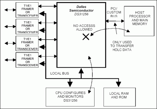
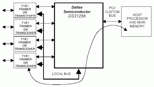
This application note describes an example of how to configure a single T3 port for unchannelized operation on the DS31256 in bridge mode. Additionally, this example describes how to construct, send, receive, and check a packet in loopback mode on that port. This application note is presented as a coding example for easy adaptation to end-user applications.The DS31256 local bus can operate in two modes :
- PCI Bridge Mode
- Configuration Mode
This example has the following configuration:
- Port 1 of the DS31256 is operated as an unchannelized port. That is, the port gets receive/transmit clocks but no sync pulse. All other ports are not used.
- HDLC channel 0 is assigned to port 1 of the DS31256. It also is assigned 256 RX FIFO blocks, 256 TX FIFO blocks, an RX FIFO high watermark of 179 (70% of 256), and a TX low watermark of 77 (30% of 256).
- Ten 16-byte packets are constructed in host memory using 10 TX buffers, 10 TX descriptors, and one TX pending-queue entry. The TX pending-queue entry points to a descriptor, which is chained to 10 descriptors via the next-descriptor pointer-field and the EOF and CV being set.
- Since the DS31256 is in loopback mode, the packet, when transmitted, also will be received by the DS31256. The received packet is written to host memory using 10 RX buffers, 10 RX descriptors, and 10 RX done-queue entries.
- The host memory is configured as follows:
- Receive Side
- RX free queue base address (RFQBA1/0) = 0x10000000
- RX done queue base address (RDQBA1/0) = 0x10000B00
- RX descriptor base address (RDBA1/0) = 0x10001080
- RX buffer base address = 0x10002680
- Transmit Side
- TX pending queue base address (TPQBA1/0) = 0x10059084
- TX done queue base address (TDQBA1/0) = 0x10059604
- TX descriptor base address (TDBA1/0) = 0x10059B84
- TX buffer base address = 0x1005B184
- Receive Side
Definition Of The Coding Example Function Calls
To improve readability, the code in this example uses several function calls. The definitions of these functions are as follows:- write_reg(address, data)
- Write the specified data to the specified DS31256 register address
- Inputs:
- address = the register address where data is to be written
- data = the data to be written to the specified register
- Outputs : None
- read_reg(address, data)
- Read the contents of the DS31256 register at the specified address
- Inputs:
- address = the register address which is to be read
- Outputs:
- data = the value read from the register
- write_reg_IS(address, data)
- Write the specified data to the specified DS31256 indirect-select register and then wait for that register's busy bit to clear before returning
- Inputs:
- address = the indirect select register where data is to be written
- data = the data to be written to the specified register
- Outputs : None
- Function Code : write_reg(address, data);
- bit_check = 0x8000;
- while (bit_check & 0x8000)
- read_reg(address, bit_check);
- wr_dword(address, data)
- Write the specified 32-bit data value to the specified 32-bit host memory address
- Inputs:
- address = the host memory address where data is to be written
- data = the data to be written to the specified memory address
- Outputs : None
- rd_dword(address, data)
- Read a 32-bit data value from the specified 32-bit host memory address
- Inputs:
- address = the host memory address that is to be read
- Outputs:
- data = the 32-bit data value read from host memory
- frame_wait(count)
- Provides a delay equal to count number of frame periods, where a frame period is 125μs
- Inputs:
- count = number of frame periods to wait
- Outputs : None
- Write the specified data to the specified DS31256 register address
Unchannelized Configuration Mode Coding Example
This coding example consists of the following steps:- Reset the DS31256
- Configure the DS31256
- Enable the HDLC channel
- Put the HDLC channel in loopback mode
- Queue, send, receive, and check a data packet
Reset the DS31256
Resetting the DS31256 consists of two steps. First, the internal RAMs of the DS31256 must be zeroed and then the DS31256 internal registers must be reset.
Zero the DS31256 Internal RAM's
The DS31256 internal configuration RAMs are not cleared by resetting the chip and, therefore, must be manually zeroed. This task is accomplished by performing a series of writes to each internal ram in the DS31256 using the appropriate data and indirect select registers of the DS31256. This section details the procedure for accomplishing this task.
| Acronym | Offset/ Address | Register Name | Data Sheet Section |
| CP[n]RDIS | 03xx | Channelized Port n Register Data Indirect Select | 6.3 |
| CP[n]RD | 03xx | Channelized Port n Register Data | 6.3 |
/* Zero RX configuration and TX configuration RAMs for all ports */
for(port = 0; port < 16; port = port + 1)
{
  write_reg(CP0RD + 8*port, 0x0000);
  for(ds0 = 0; ds0 < 128; ds0 = ds0 + 1)
  {
  	/* Set bits 9-8 = 01 to select RX Configuration RAM */
  	/* Set bits 9-8 = 10 to select TX Configuration RAM */
  	write_reg_IS(CP0RDIS + 8*port, (0x0100 + ds0));
  	write_reg_IS(CP0RDIS + 8*port, (0x0200 + ds0));
  }
}
| Acronym | Offset/ Address | Register Name | Data Sheet Section |
| RHCDIS | 0400 | Receive HDLC Channel Definition Indirect Select | 7.2 |
| RHCD | 0404 | Receive HDLC Channel Definition | 7.2 |
/* Zero the RX HDLC Channel Definition RAM */
write_reg(RHCD, 0x0000);
for(channel = 0; channel < 256; channel = channel + 1)
  write_reg_IS(RHCDIS, channel);
| Acronym | Offset/ Address | Register Name | Data Sheet Section |
| THCDIS | 0480 | Transmit HDLC Channel Definition Indirect Select | 7.2 |
| THCD | 0484 | Transmit HDLC Channel Definition | 7.2 |
/* Zero the TX HDLC Channel Definition RAM */
write_reg(THCD, 0x0000);
for(channel = 0; channel < 256; channel = channel + 1)
  write_reg_IS(THCDIS, channel);
| Acronym | Offset/ Address | Register Name | Data Sheet Section |
| RFSBPIS | 0900 | Receive FIFO Staring Block Pointer Indirect Select | 8.2 |
| RFSBP | 0904 | Receive FIFO Starting Block Pointer | 8.2 |
/* Zero the RX FIFO Starting Block Pointer RAM */
write_reg(RFSBP, 0x0000);
for(channel = 0; channel < 256; channel = channel + 1)
  write_reg_IS(RFSBPIS, channel);
| Acronym | Offset/ Address | Register Name | Data Sheet Section |
| RFBPIS | 0910 | Receive FIFO Block Pointer Indirect Select | 8.2 |
| RFBP | 0914 | Receive FIFO Block Pointer | 8.2 |
/* Zero the RX FIFO Block Pointer RAM  */
write_reg(RFBP, 0x0000);
for(channel = 0; channel < 256; channel = channel + 1)
  write_reg_IS(RFBPIS, channel);
| Acronym | Offset/ Address | Register Name | Data Sheet Section |
| RFHWMIS | 0920 | Receive FIFO High Watermark Indirect Select | 8.2 |
| RFHWM | 0924 | Receive FIFO High Watermark | 8.2 |
/* Zero the RX FIFO High Watermark RAM  */
write_reg(RFHWM, 0x0000);
for(channel = 0; channel < 256; channel = channel + 1)
  write_reg_IS(RFHWMIS, channel);
| Acronym | Offset/ Address | Register Name | Data Sheet Section |
| TFSBPIS | 0980 | Transmit FIFO Starting Block Pointer Indirect Select | 8.2 |
| TFSBP | 0984 | Transmit FIFO Starting Block Pointer | 8.2 |
/* Zero the TX FIFO Starting Block Pointer Registers */
write_reg(TFSBP, 0x0000);
for(channel = 0; channel < 256; channel = channel + 1)
  write_reg_IS(TFSBPIS, channel);
| Acronym | Offset/ Address | Register Name | Data Sheet Section |
| TFBPIS | 0990 | Transmit FIFO Block Pointer Indirect Select | 8.2 |
| TFBP | 0994 | Transmit FIFO Block Pointer | 8.2 |
/* Zero the TX FIFO Block Pointer RAM */
write_reg(TFBP, 0x0000);
for(channel = 0; channel < 256; channel = channel + 1)
  write_reg_IS(TFBPIS, channel);
| Acronym | Offset/ Address | Register Name | Data Sheet Section |
| TFLWMIS | 09A0 | Transmit FIFO Block Pointer Indirect Select | 8.2 |
| TFLWM | 09A4 | Transmit FIFO Low Watermark | 8.2 |
/* Zero the TX FIFO Low Watermark RAM */
write_reg(TFLWM, 0x0000);
for(channel = 0; channel < 256; channel = channel + 1)
  write_reg_IS(TFLWMIS, channel);
| Acronym | Offset/ Address | Register Name | Data Sheet Section |
| RDMACIS | 0770 | Receive DMA Configuration Indirect Select | 9.3.5 |
| RDMAC | 0774 | Receive DMA Configuration | 9.3.5 |
/* Zero the RX DMA Configuration RAM */
write_reg(RDMAC, 0x0000);
for(channel = 0; channel < 256; channel = channel + 1)
  write_reg_IS(RDMACIS, 0x0400 + channel);
| Acronym | Offset/ Address | Register Name | Data Sheet Section |
| TDMACIS | 0870 | Transmit DMA Configuration Indirect Select | 8.2.5 |
| TDMAC | 0874 | Transmit DMA Configuration | 8.2.5 |
/* Zero the TX DMA Configuration RAM */
write_reg(TDMAC, 0x0000);
for(channel = 0; channel < 256; channel = channel + 1)
  write_reg_IS(TDMACIS, 0x0400 + channel);
Reset the DS31256 Internal Registers
A software reset can be performed on all registers in the DS31256 using the master reset register (MRID). The host must set this bit back to 0 before the device can be programmed for normal operation.
| Acronym | Offset/ Address | Register Name | Data Sheet Section |
| MRID | 0000 | Master Reset & ID Register | 5.1 |
/* Reset DS31256 using MRID registers master reset bit. */
write_reg(MRID, 0x0001);
write_reg(MRID, 0x0000);
Configure the DS31256
Configuration of the DS31256 consists of the following steps:- Configure the PCI registers
- Configure the Layer 1 registers
- Configure the HDLC registers
- Configure the FIFO registers
- Configure the DMA registers
/* This example uses port 1 channel 0 */
port = 1;
channel = 0;

/* RX free queue base address */
rfq_base_addr = 0x10000000;

/* RX free queue end address */
/* RX free queue size = 16 */
rfq_end_idx = 0x000F;

/* RX done queue base address */
rdq_base_addr = 0x10000B00;

/* RX done queue end address */
/* RX done queue size = 16 */
rdq_end_idx = 0x000F;

/* RX descriptor base address */
/* RX descriptor table size = 256 */
rdscr_base_addr = 0x10001080;

/* RX data buffer base address */
rx_buf_base_addr = 0x10002680;

/* TX pending queue base address */
tpq_base_addr = 0x10059084;

/* TX pending queue end address */
/* TX pending queue size = 16 */
tpq_end_idx = 0x000F;

/* TX done queue base address */
tdq_base_addr = 0x10059604;

/* TX done queue end address */
/* TX done queue size = 16 */
tdq_end_idx = 0x000F;

/* TX descriptor base address */
/* TX descriptor table size = 256 */
tdscr_base_addr = 0x10059B84;

/* TX data buffer base address */
tx_buf_base_addr = 0x1005B184;
Configure the PCI Registers
The PCI bridge mode allows the host on the PCI bus to access the local bus. The PCI bus is used to control and monitor the DS31256 and transfer the packet data. The DS31256 will map data from the PCI bus to the local bus. (Refer to Section 10 of the DS31256 data sheet.)
| Acronym | Offset/ Address | Register Name | Data Sheet Section |
| PCMD0 | 0x004/0A04 | PCI Command Status 0 | 10.2 |
/* Map DS31256 configuration registers to a PCI Bus Base Address */
write_reg(PDCM, 0x80000000);

/* PCI command/status register 0 - controls DS31256 DMA functionality */
/* Set bit 1 = 1 to enable accesses to internal device configuration registers through PCI bus (required for bridge mode) */
/* Set bit 2 = 1 to allow the device operation as bus master on PCI bus (required for DMA) */
/* Set bit 6 = 1 to act on parity errors */
/* Set bit 8 = 1 to enable the PSERR pin */
write_reg(PCMD0, 0x00000146);
Configure the Layer 1 Registers
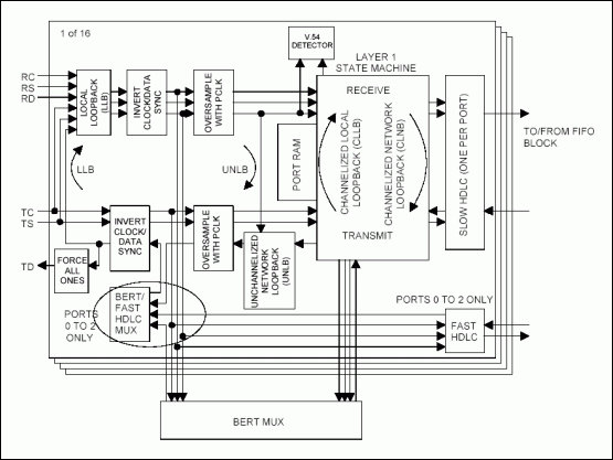
Each port of the DS31256 contains a Layer 1 controller that performs several functions including:- Assigning the HDLC channel number to the incoming and outgoing data
- Channelized local and network loopbacks
- Channelized selection of 64kbps, 56kbps, or no data
- Channelized transmit DS0 channel fill of all ones
- Routing data to and from the BERT function
- Routing data to the V.54 loop pattern detector
| Acronym | Offset/ Address | Register Name | Data Sheet Section |
| RP[n]CR | 01xx | Receive Port n Control Register | 6.2 |
| TP[n]CR | 02xx | Transmit Port n Control Register | 6.2 |
| CP[n]RDIS | 03xx | Channelized Port n Register Data Indirect Select | 6.3 |
| CP[n]RD | 03xx | Channelized Port n Register Data | 6.3 |
/* Set RX Port Control Register */
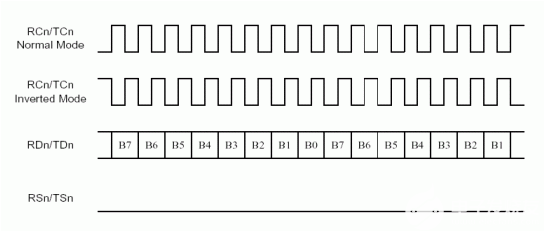
/* Set bits 2-0 = 000 for clock, data and sync are not inverted */
/* Set bits 5-4 = 00 for sync pulse 0 clocks early */
/* Bits 7-6 are ignored; the high-speed mode is enabled   */
/* Set bit 8 = 1 to enable high-speed mode */
/* Set bit 9 = 1 to enable unchannelized mode */
/* Set bit 10 = 0 to disable local loopback */
/* Bit 11 is not assigned */
/* Bits 12-13 are read only */
/* Set bit 14 = 0 to enable unchannelized mode */
/* Bit 15 is read only */
write_reg(RP0CR + 4*port, 0x0300);
/* Set TX Port Control Register */
/* Set bit 2-0 = 000 for clock, data and sync are not inverted */
/* Set bit 3 = 0 to force all data at TD to be 1 */
/* Set bits 5-4 = 00 for sync pulse 0 clocks early */
/* Bits 7-6 are ignored when the high-speed mode is enabled (TUEN=1)  */
/* Set bit 8 = 1 to enable high-speed mode */
/* Set bit 9 = 1 to enable unchannelized mode */
/* Set bit 10 = 0 to disable network loopback */
/* Set bit 11 = 0 to select source transmit data from the HDLC controller */
/* Bits 12-13 is not assigned */
/* Set bit 14 = 0 to mask interrupt */
/* Bit 15 is read only */
write_reg(TP0CR + 4*port, 0x0300);
Configure the HDLC Registers
The DS31256 contains a 256-channel HDLC controller that performs the Layer 2 functions, which include the following:- Zero stuffing and destuffing
- Flag detection and byte alignment
- CRC generation and checking
- Data inversion and bit flipping
| Acronym | Offset/ Address | Register Name | Data Sheet Section |
| RHCDIS | 0400 | Receive HDLC Channel Definition Indirect Select | 7.2 |
| RHCD | 0404 | Receive HDLC Channel Definition | 7.2 |
| THCDIS | 0480 | Transmit HDLC Channel Definition Indirect Select | 7.2 |
| THCD | 0484 | Transmit HDLC Channel Definition | 7.2 |
/* RX HDLC configuration */
/* Set bits 3-2 = 10 for 32-bit CRC */
write_reg(RHCD, 0x0008);
write_reg_IS(RHCDIS, channel);

/* TX HDLC Configuration */
/* Set bit 1= 0 to select an interfill byte of 7E */
/* Set bits 3-2 = 10 for 32-bit CRC */
/* Set bits 11-8 = 0000 share closing and opening flag */
write_reg(THCD, 0x0008);
write_reg_IS(THCDIS, channel);
Configure the FIFO Registers
The DS31256 contains a 16kbyte transmit FIFO and a 16kbyte receive FIFO. Each FIFO is divided into 1024 blocks of four double words (dwords) or 16 bytes. FIFO memory is allocated on an HDLC channel basis. The amount of FIFO memory allocated to each HDLC channel is programmable and can be a minimum of four blocks and a maximum of 1024 blocks. FIFO memory is allocated to HDLC channels by creating a circular-linked list out of a group of blocks, where each block points to the next block in the chain and the last block points to the first. The FIFO block-linked list is assigned to a specific HDLC channel by assigning one block in the linked list to be that channel's FIFO starting block pointer.In this example, 256 TX FIFO blocks and 256 RX FIFO blocks are assigned to the HDLC channel. This example also uses an RX FIFO high watermark of 179 and TX FIFO low watermark of 77. The RX FIFO high watermark indicates how many blocks should be written into RX FIFO by the HDLC engines before the DMA will begin sending the data to the PCI Bus. The high watermark setting must be between one block and one less than the number of blocks in the link-list chain for the particular channel involved. The TX FIFO low watermark indicates how many blocks should be left in the TX FIFO before the DMA should begin getting more data from the PCI Bus. The amount of FIFO memory, RX FIFO high watermark, and TX FIFO low watermark required by an HDLC channel to prevent transmit underflows and receive overflows from occurring is application-dependent. Note that watermark selection often needs to be optimized, and is very application-dependent. In general, setting both the high and low watermarks at 50% is a good starting point. Finally, the TX FIFO and RX FIFO of the DS31256 are configured independently on an HDLC channel basis via the registers listed in the following tables.
| Acronym | Offset/ Address | Register Name | Data Sheet Section |
| RHCDIS | 0910 | RFBPIS Receive FIFO Block Pointer Indirect Select | 7.2 |
| RHCD | 0914 | RFBP Receive FIFO Block Pointer | 7.2 |
/* Build the RX FIFO block linked list  0->1->2->3->4 ... 255 -> 0 */
for (block = 0; block < 255; block = block + 1)
{
/* Bits 9-0 in RFBP register indicate which block is next in the linked list */
write_reg(RFBP, block + 1);
write_reg_IS(RFBPIS, block);
}

/* The last block points to the first block to create a circular linked list */
write_reg(RFBP, 0x0000);
write_reg_IS(RFBPIS, 0x00FF);

/* Assign the circular linked list to a specific channel */
write_reg(RFSBP, 0x0000);
write_reg_IS(RFSBPIS, channel);
| Acronym | Offset/ Address | Register Name | Data Sheet Section |
| RFHWMIS | 0920 | Receive FIFO High Watermark Indirect Select | 8.2 |
| RFHWM | 0924 | Receive FIFO High Watermark | 8.2 |
/* Set RX FIFO high watermark for channel to 179 */
write_reg(RFHWM, 0x00B3);
write_reg_IS(RFHWMIS, channel);
| Acronym | Offset/ Address | Register Name | Data Sheet Section |
| TFBPIS | 0990 | Transmit FIFO Block Pointer Indirect Select | 8.2 |
| TFBP | 0994 | Transmit FIFO Block Pointer | 8.2 |
/* TX FIFO block linked list 0->1->2->3->4 ... 255->0 */
for(block = 0; block < 255; block = block + 1)
{
/* Bits 9-0 in RFBP register indicate which block is next in the linked list */
write_reg(TFBP, block + 1);
write_reg_IS(TFBPIS, block);
}

/* The last block points to the first block to create a circular linked list */
write_reg(TFBP, 0x0000);
write_reg_IS(TFBPIS, 0x00FF);
| Acronym | Offset/ Address | Register Name | Data Sheet Section |
| TFSBPIS | 0980 | Transmit FIFO Starting Block Pointer Indirect Select | 8.2 |
| TFSBP | 0984 | Transmit FIFO Starting Block Pointer | 8.2 |
/* Assign the circular linked list to a specific channel */
write_reg(TFSBP, 0x0000);
write_reg_IS(TFSBPIS, channel);

/* Set TX FIFO low watermark for channel to 77 */
write_reg(TFLWM, 0x004D);
write_reg_IS(TFLWMIS, channel);
Configure the DMA Registers
The DMA block handles the transfer of packet data from the FIFO block to the PCI block and vice versa. The PCI block controls data transfers between the DS31256 and the external PCI bus. The host, defined as the CPU or intelligent controller that sits on the PCI bus, instructs the DS31256 about how to handle the incoming and outgoing data.This is accomplished using descriptors that are defined as preformatted messages passed from the host to the DMA block or vice versa. Via these descriptors, the host informs the DMA about the location and status of packet data to be transmitted, and where to place packet data that is received. The DMA uses these descriptors to tell the host the status of packet data that has been transmitted and the status and location of packet data that has been received.
On the receive side, the host will write to the free queue descriptors, informing the DMA where it can place incoming packet data. Associated with each free queue entry is a receive-data buffer location and packet descriptor. As the DS31256 uses receive-free queue entries to write received packet data to host memory it creates entries in the RX done queue. These RX done-queue entries inform the host about the location and status of received data. Refer to the DS31256 data sheet for more detailed information. The host must configure the RX DMA by writing to all of the registers in the following table:
| Acronym | Offset/ Address | Register Name | Data Sheet Section |
| RFQBA0 | 0700 | Receive Free Queue Base Address 0 (lower word) | 9.2.3 |
| RFQBA1 | 0704 | Receive Free Queue Base Address 1 (upper word) | 9.2.3 |
| RFQEA | 0708 | Receive Free Queue end Address | 9.2.3 |
| RFQSBSA | 070C | Receive Free Small Buffer Start Address | 9.2.3 |
| RFQLBWP | 0710 | Receive Free Queue Large Buffer Host Write Pointer | 9.2.3 |
| FQSBWP | 0714 | Receive Free Queue Small Buffer Host Write Pointer | 9.2.3 |
| RFQLBRP | 0718 | Receive Free Queue Large Buffer DMA Read Pointer | 9.2.3 |
| RFQSBRP | 071C | Receive Free Queue Small Buffer DMA Read Pointer | 9.2.3 |
| RDQBA0 | 0730 | Receive Done Queue Base Address 0 (lower word) | 9.2.4 |
| RDQBA1 | 0734 | Receive Done Queue Base Address 1 (upper word) | 9.2.4 |
| RDQEA | 0738 | Receive Done Queue end Address | 9.2.4 |
| RDQRP | 073C | Receive Done Queue Host Read Pointer | 9.2.4 |
| RDQWP | 0740 | Receive Done Queue DMA Write Pointer | 9.2.4 |
| RDBA0 | 0750 | Receive Descriptor Base Address 0 (lower word) | 9.2.2 |
| RDBA1 | 0754 | Receive Descriptor Base Address 1 (upper word) | 9.2.2 |
| RDMACIS | 0770 | Receive DMA Configuration Indirect Select | 9.3.5 |
| RDMAC | 0774 | Receive DMA Configuration | 9.3.5 |
| RLBS | 0790 | Receive Large Buffer Size | 9.2.1 |
/* RX large buffer size = 256 bytes */
write_reg(RLBS, 0x0100);

/* RX free queue base address */
write_reg(RFQBA0, rfq_base_addr & 0x0000FFFF);
write_reg(RFQBA1, (rfq_base_addr >> 16) & 0x0000FFFF);

/* RX free queue large buffer read and write pointers = 0 */
write_reg(RFQLBRP, 0x0000);
write_reg(RFQLBWP, 0x0000);

/* RX free queue small buffer start address = 16 */
write_reg(RFQSBSA, rfq_end_idx);
/* RX free queue small buffer read and write pointers = 0 */
write_reg(RFQSBRP, 0x0000);
write_reg(RFQSBWP, 0x0000);

/* RX free queue end address */
write_reg(RFQEA, rfq_end_idx);

/* RX done queue base address */
write_reg(RDQBA0, rdq_base_addr & 0x0000FFFF);
write_reg(RDQBA1, (rdq_base_addr >> 16) & 0x0000FFFF);

/* RX done queue read and write pointers = 0 */
write_reg(RDQRP, 0x0000);
write_reg(RDQWP, 0x0000);

/* RX done queue end address */
write_reg(RDQEA, rdq_end_idx);

/* RX descriptor base address */
write_reg(RDBA0, rdscr_base_addr & 0x0000FFFF);
write_reg(RDBA1, (rdscr_base_addr >> 16) & 0x0000FFFF);

/* RX DMA Channel Configuration */
/* The data in RDMAC register is written to or read from the Receive Configuration RAM */
/* Set bit 0 = 0 to disable the HDLC Channel */
/* Set bit 2-1 = 00 for large buffers only */
/* Set bit 6-3 = 0000 for 0 byte offset from the data buffer address of the first data buffer */
/* Set bit 9-7 = 000 for DMA write to the done queue only after packet reception is complete */
/* Set the HDLC channel number by RDMACIS register */
write_reg(RDMAC, 0x0000);
write_reg_IS(RDMACIS, 0x0400 + channel);
On the transmit side, the host will write to the pending queue, informing the DMA which channels have packet data that is ready to be transmitted. Associated with each pending-queue descriptor is a linked list of one or more transmit-packet descriptors that describe the packet data. Each of these transmit-packet descriptors also has a pointer to a transmit-data buffer that contains the actual data payload of the HDLC packet.
As the DS31256 processes transmit-pending queue-descriptor entries, it creates transmit-done queue-descriptor queue entries. The DMA will write to the done queue when it has completed transmitting either a complete packet or data buffer depending on how the DS31256 is configured. Via these done-queue descriptors, the DMA informs the host about the status of the outgoing packet data. Refer to the DS31256 data sheet for more detailed information. The host must configure the TX DMA by writing to all of the registers in the following table:
| Acronym | Offset/ Address | Register Name | Data Sheet Section |
| TPQBA0 | 0800 | Transmit Pending Queue Base Address 0 (lower word) | 9.3.3 |
| TPQBA1 | 0804 | Transmit Pending Queue Base Address 1 (upper word) | 9.3.3 |
| TPQEA | 0808 | Transmit Pending Queue end Address | 9.3.3 |
| TPQWP | 080C | Transmit Pending Queue Host Write Pointer | 9.3.3 |
| TPQRP | 0810 | Transmit Pending Queue DMA Read Pointer | 9.3.3 |
| TDQBA0 | 0830 | Transmit Done Queue Base Address 0 (lower word) | 9.3.4 |
| TDQBA1 | 0834 | Transmit Done Queue Base Address 1 (upper word) | 9.3.4 |
| TDQEA | 0838 | Transmit Done Queue end Address | 9.3.4 |
| TDQRP | 083C | Transmit Done Queue Host Read Pointer | 9.3.4 |
| TDQWP | 0840 | Transmit Done Queue DMA Write Pointer | 9.3.4 |
| TDBA0 | 0850 | Transmit Descriptor Base Address 0 (lower word) | 9.3.2 |
| TDBA1 | 0854 | Transmit Descriptor Base Address 1 (upper word) | 9.3.2 |
| TDMACIS | 0870 | Transmit DMA Configuration Indirect Select | 9.3.5 |
| TDMAC | 0874 | Transmit DMA Configuration | 9.3.5 |
/* TX pending queue base address */
write_reg(TPQBA0, tpq_base_addr & 0x0000FFFF);
write_reg(TPQBA1, (tpq_base_addr >> 16) & 0x0000FFFF);

/* TX pending queue read and write pointers = 0 */
write_reg(TPQRP, 0x0000);
write_reg(TPQWP, 0x0000);

/* TX pending queue end address */
write_reg(TPQEA, tpq_end_idx);

/* TX done queue base address */
write_reg(TDQBA0, tdq_base_addr & 0x0000FFFF);
write_reg(TDQBA1, (tdq_base_addr >> 16) & 0x0000FFFF);

/* TX done-queue read and write pointers = 0 */
write_reg(TDQRP, 0x0000);
write_reg(TDQWP, 0x0000);

/* TX done-queue end address */
write_reg(TDQEA, tdq_end_idx);

/* TX descriptor base address */
write_reg(TDBA0, tdscr_base_addr & 0x0000FFFF);
write_reg(TDBA1, (tdscr_base_addr >> 16) & 0x0000FFFF);

/* TX DMA Channel Configuration */
/* The data in TDMAC register is written to or read from the Receive Configuration RAM */
/* Set bit 0 = 0 to disable HDLC Channel */
/* Set bit 1 = 0 for write done queue after packet transmitted */
/* Set the HDLC Channel Number by TDMACIS register */
write_reg(TDMAC, 0x0000);
write_reg_IS(TDMACIS, 0x0200 + channel);
Enable the HDLC Channel
The next step after the DS31256 has been initialized is to enable the HDLC channel. In addition to the configuration steps already described, the following steps must be performed to enable packet transmission and reception in the DS31256:- Enable the channel in the port TX and RX configuration RAMs
- Enable port data transmission in Layer 1
- Enable TX DMA and RX DMA for the DS31256
- Enable HDLC channel TX DMA and RX DMA
| Acronym | Offset/Address | Register Name | Data Sheet Section |
| MC | 0010 | Master Configuration Register | 5.2 |
| TP[n]CR | 02xx | Transmit Port n Control Register | 6.2 |
| RDMACIS | 0770 | Receive DMA Configuration Indirect Select Register | 9.3.5 |
| RDMAC | 0774 | Receive DMA Configuration Register | 9.3.5 |
| TDMACIS | 0870 | Transmit DMA Configuration Indirect Select Register | 9.3.5 |
| TDMAC | 0874 | Transmit DMA Configuration Indirect Select Register | 9.3.5 |
/* TX port control register */
/* Set bit 3 = 1 to allow data to be transmitted normally */
read_reg(TP0CR + 4*port, data);
write_reg(TP0CR + 4*port, data | 0x0008);

/* Enable TX and RX DMA in the DS31256 master configuration register */
/* Set bit 0 = 1 to enable Receive DMA */
/* Set bits 2-1 = 00 to burst length maximum is 32 dwords.  The optimum length */
/*                                       is application-dependent. */
/* Set bit 3 = 1 to enable Transmit DMA */
/* Set bit 6 = 1 for HDLC packet data on PCI bus is big endian */
/* Set bits 11-7 = 00000 to give Port 0 the dedicated resources of the BERT */
write_reg(MC, 0x0049);

/* Read the current channel value from the RX DMA Configuration RAM */
/* Set RDMACIS bits 7-0 = channel */
/* Set RDMACIS bits 10-8 = 100 to read lower word of dword 2 */
/* Set RDMACIS bit 14 = 1 to read from RAM */
write_reg_IS(RDMACIS, 0x4400 + channel);
read_reg(RDMAC, data);

/* Enable channel RX DMA */
/* Update RAM with new value */
/* Set RDMAC bit 0 = 1 to enable the HDLC channel */
/* Set RDMACIS bits 7-0 = channel */
/* Set RDMACIS bits 10-8 = 100 to write lower word of dword 2 */
/* Set RDMACIS bit 14 = 0 to write to RAM */
write_reg(RDMAC, data | 0x0001);
write_reg_IS(RDMACIS, 0x0400 + channel);

/* Read the current channel value from the TX DMA Configuration RAM */
/* Set TDMACIS bits 7-0 = channel */
/* Set TDMACIS bits 11-8 = 0010 to read lower word of dword 1 */
/* Set TDMACIS bit 14 = 1 to read from RAM */
write_reg_IS(TDMACIS, 0x4200 + channel);
read_reg(TDMAC, data);

/* Enable channel TX DMA */
/* Update RAM with new value */
/* Set TDMAC bit 0 = 1 to enable the HDLC channel */
/* Set TDMACIS bits 7-0 = channel */
/* Set TDMACIS bits 11-8 = 0010 to write lower word of dword 1 */
/* Set TDMACIS bit 14 = 0 to write to RAM */
write_reg((TDMAC, data | 0x0001);
write_reg_IS(TDMACIS, 0x0200 + channel);
Put the HDLC Channel in Loopback Mode
After the channel has been configured and enabled it takes approximately five frame periods, or 625μs, for the internal logic of the DS31256 to complete the transition to the new configuration. Once this transition has completed the HDLC channel then can be placed in loopback mode so that all data transmitted on the channel also will be received on that channel. Placing the HDLC channel in loopback mode prior to the five-frame wait period can result in writing garbage data into the channel's RX FIFO.
| Acronym | Offset/ Address | Register Name | Data Sheet Section |
| RP[n]CR | 01xx | Receive Port n Control Register | 6.2 |
/* Wait for at least five frame periods for the internal DS31256 initialization to complete */
frame_wait(5);

/* Set bit 10 = 1 to enable loopback - routes transmit data back to the receive port */
read_reg(RP0CR + 4*port, data);
write_reg(RP0CR + 4*port, data | 0x0400);
Queue, Send, Receive, and Check a Data Packet
Once the DS31256 initialization has been completed data can be transmitted and received. Since the DS31256 is in loopback mode all data transmitted on the HDLC channel will also be received on that channel. This section describes the process of how to build a data packet in host memory, transmit and receive the packet, and check the results. The following sections describe this process in detail.
Initialize the RX Free Queue
Before the DS31256 can transfer received packets from its internal FIFO to host memory, the host must instruct the DS31256 where to put the data. This is done via the RX free queue. Each entry in the RX free queue contains a pointer to an RX data buffer and an RX packet descriptor index. This example uses 10 RX free queue entries. Each entry contains one RX free queue large buffer and one RX packet descriptor. The DS31256 RX large data buffer size has been set to 256 bytes (RLBS = 256). Additionally, the DS31256 has been configured to use a 4-byte CRC and to write the RX CRC into the RX data buffer. Therefore, one RX large data buffer is capable of holding up to 252 bytes of packet data.
| Acronym | Offset/ Address | Register Name | Data Sheet Section |
| RFQLBWP | 0710 | Receive Free Queue Large Buffer Host Write Pointer | 9.2.3 |
| RFQLBRP | 0718 | Receive Free Queue Large Buffer DMA Read Pointer | 9.2.3 |
/* check for space in RX large free queue */
read_reg(RFQLBWP, wr_ptr);
read_reg(RFQLBRP, rd_ptr);
if (rd_ptr > wr_ptr)
cnt = rd_ptr - wr_ptr - 1;
else
cnt = rfq_end_idx - wr_ptr + rd_ptr;

/* If room in RX free queue then put 10 entries in the queue */
/* dword 0 = RX data buffer address */
/* (use RX data buffer starting at RX buffer area base address) */
/* dword 1 = corresponding RX descriptor index (use RX descriptor table index 0) */
if (cnt > 9)
{
rx_dscr_idx = 0;
for (index=0, index <10, index++)
{
wr_dword(rfq_base_addr + wr_ptr*8, rx_buf_base_addr+index*256);
wr_dword(rfq_base_addr + wr_ptr*8+4, index);
if (wr_ptr == rfq_end_idx)
wr_ptr = 0;
else
wr_ptr++;
}
/* Advance the RX free queue large buffer write pointer by 10 */
write_reg(RFQLBWP, wr_ptr);
}
Build the Packet in Host Memory
This example will send a chain of 10 16-byte data packets. Before a packet can be sent it must be constructed in the host memory. Additionally, a corresponding TX packet descriptor also must be constructed in host memory. Each of these tasks is detailed in the following code./* Create a 16-byte data packet in memory in a TX buffer whose start address is the TX buffer area base address */
wr_dword(tx_buf_base_addr, 0x01234567);
wr_dword(tx_buf_base_addr + 4, 0x89ABCDEF);
wr_dword(tx_buf_base_addr + 8, 0x02468ACE);
wr_dword(tx_buf_base_addr + 12, 0x13579BDF);
/* Second data packet goes in second data buffer (16-byte packet in 256-byte buffer). */
wr_dword(tx_buf_base_addr + 256, 0x08192A3B);
wr_dword(tx_buf_base_addr + 256 + 4, 0x4D5E6F70);
wr_dword(tx_buf_base_addr + 256 + 8, 0x8192A3B4);
wr_dword(tx_buf_base_addr + 256 + 12, 0xC5D6E7F8);
/* Create 8 more packets with unique data in each. */
for (index = 2, index < 10, index++)
{
wr_dword(tx_buf_base_addr + index*256, 0x08192A30 + index);
wr_dword(tx_buf_base_addr + index*256 + 4, 0x4D5E6F71 + index);
wr_dword(tx_buf_base_addr + index*256 + 8, 0x8192A3B2 + index);
wr_dword(tx_buf_base_addr + index*256 + 12, 0xC5D6E7F3 + index);
}
Create 10 TX Descriptors (4 dwords each)
/* TX descriptor table index 0 */
/* dword0 = TX buffer address */
/* dword1 = EOF, CV, byte count (10h), next descriptor pointer */
/* dword2 = HDLC channel */
/* dword3 = PV, next pending descriptor pointer (set to 0) */
tx_dscr_idx = 0;
for (index = 0, index < 10, index++)
{
wr_dword(tdscr_base_addr + index*16, tx_buf_base_addr+index*256);
if (index == 9)
wr_dword(tdscr_base_addr + index*16 + 4, 0x80100000);
/* end of chain, CV set to 0 */
else
wr_dword(tdscr_base_addr + index*16 + 4, 0xC0100000 + index+1);
wr_dword(tdscr_base_addr + index*16 + 8, 0x00000000 + channel);
wr_dword(tdscr_base_addr + index*16 + 12, 0x00000000);
}
/* This creates 10 TX descriptors that are chained or linked together via the next descriptor pointer. */
Transmit and Receive the Packet
To transmit the packets, the TX descriptor must be placed in the transmit-pending queue and then the transmit-pending queue-write pointer (TPQWP) must be incremented. When the DS31256 detects that the pending queue is not empty (TPQWP not equal to TPQRP) it will begin processing queue entries and the packet will be transmitted.
| Acronym | Offset/ Address | Register Name | Data Sheet Section |
| SDMA | 0028 | Status Register for DMA | 5.3.2 |
| TPQWP | 080C | Transmit Pending Queue Host Write Pointer | 9.3.3 |
| TPQRP | 0810 | Transmit Pending Queue DMA Read Pointer | 9.3.3 |
/* Read SDMA register to clear any previously set status bits */
read_reg(SDMA, data);

Write the TX Pending-Queue Entry
/* check free space in TX pending queue */
read_reg(TPQWP, wr_ptr);
read_reg(TPQRP, rd_ptr)
if (rd_ptr > wr_ptr)
cnt = rd_ptr - wr_ptr - 1;
else
cnt = rfq_end_idx - wr_ptr + rd_ptr;

/* If room in the TX pending queue create an entry for the packet */
if (cnt > 0)
{
/* Bits 0-15 Descriptor Pointer (0000h) */
/* Bits 16-23 HDLC channel - (channel << 16) */
wr_dword(tpq_base_addr + wr_ptr*4, 0x0000000 + (channel << 16));

/* Advance the TX pending-queue write pointer */
if (wr_ptr == tpq_end_idx)
wr_ptr = 0;
else
wr_ptr = wr_ptr + 1;
write_reg(TPQWP, wr_ptr);
}
Check the Results
After waiting a sufficient period of time for the packet to be transmitted and received, several checks can be performed to determine if packet transmission and reception was successful. The following code details these checks.
| Acronym | Offset/ Address | Register Name | Data Sheet Section |
| SDMA | 0028 | Status Register for DMA | 5.3.2 |
| RFQLBWP | 0710 | Receive Free Queue Large Buffer Host Write Pointer | 9.2.3 |
| RFQLBRP | 0718 | Receive Free Queue Large Buffer DMA Read Pointer | 9.2.3 |
| RDQRP | 073C | Receive Done Queue Host Read Pointer | 9.2.4 |
| RDQWP | 0740 | Receive Done Queue DMA Write Pointer | 9.2.4 |
| TDQRP | 083C | Transmit Done Queue Host Read Pointer | 9.3.4 |
| TDQWP | 0840 | Transmit Done Queue DMA Write Pointer | 9.3.4 |
/* Wait two frame periods for packet to be transmitted/received */
frame_wait(2);
/* Check SDMA register, Expected value = 0x6440; if not, it means there was error */
read_reg(SDMA, data);

/* Check to see how many entries are in the TX done queue (distance from TDQRP to TDQWP) */
/* Expected value is 0Ah - 10 entries in the TX done queue corresponding to the 10 packets that were sent */
read_reg(TDQRP, rd_ptr);
read_reg(TDQWP, wr_ptr);
if (wr_ptr >= rd_ptr)
cnt = wr_ptr - rd_ptr;
else
cnt = tdq_end_idx + 1 - rd_ptr + wr_ptr;

/* Check TX done-queue descriptor */
/* Expected value = 0x00000000 */
/* Bits 15-0 indicates the descriptor pointer */
/* Bits 23-16 indicate the channel number, it should be 0 in this example */
/* Bits 28-26 indicate the packet status, all 0 means the packet transmission is complete and the descriptor */
/* Pointer field corresponds to the first descriptor in the HDLC packet that has been transmitted */
for (index = 0; index < 10; index++)
{
rd_dword(tdq_base_addr + rd_ptr*4, tdq_entry);
/* Advance the TX done-queue read pointer */
if (rd_ptr == tdq_end_idx)
rd_ptr = 0;
else
rd_ptr = rd_ptr + 1;
write_reg(TDQRP, rd_ptr);
}

/* Check the RX large free queue to see how many RX buffers are in the queue (distance from RFQLBRP to RFQLBWP) */
/* Expected number is 0 since the queue had 10 buffers before the packet was received and packet reception required 10 buffers */
read_reg(RFQLBRP, rd_ptr);
read_reg(RFQLBWP, wr_ptr);
if (wr_ptr >= rd_ptr)
cnt = wr_ptr - rd_ptr;
else
cnt = rfq_end_idx + 1 - rd_ptr + wr_ptr;

/* Check RX done queue to see if any packets were received (distance from RDQRP to RDQWP)
Expected value is 10 - 10 entries in the RX done-queue entry corresponding to the 10 packets that should have been received */
read_reg(RDQRP, rd_ptr);
read_reg(RDQWP, wr_ptr);
if (wr_ptr >= rd_ptr)
cnt = wr_ptr - rd_ptr;
else
cnt = rdq_end_idx + 1 - rd_ptr + wr_ptr;

/* Check the RX done queue descriptor */
/* Expected value = 0x40000000, */
/* Bits 15-0 indicates the descriptor pointer */
/* Bits 23-16 indicate the channel number; it should be 0 in this example */
/* Bits 26-24 indicate the buffer count; all 0 means that a complete packet has been received */
/* Bit 30 EOF = 1 indicates the receiver descriptor is the last one in the chain */
for (index = 0;index < 10;index++)
/* Check all 10 entries */
{
rd_dword(rdq_base_addr + 8*rd_ptr, rdq_entry);

/* Check the corresponding RX descriptor (4 dwords) */
/* dword 0 expected value = 0x10002680 the RX buffer address */
/* dword 1 expected value = 0x80140000 */
/* Bits 15-0 is the next descriptor pointer */
/* Bits 28-16 is the number of bytes stored in the data buffer */
/* Bits 31-29 indicates buffer status */
/* dword 2 expected value = 0xxxxxxx00 */
/* Bits 7-0 indicates HDLC channel number (should match TDQ entry channel) */
/* Bits 31-8 indicates the timestamp (varies) */
rdscr_idx = rdq_entry & 0x0000FFFF;
rd_dword(rdscr_base_addr + 16*rdscr_idx, rdscr_dword0);
rd_dword(rdscr_base_addr + 16*rdscr_idx + 4, rdscr_dword1);
rd_dword(rdscr_base_addr + 16*rdscr_idx + 8, rdscr_dword2);

/* Check the data in the RX buffer */
/* 16 bytes of data + 4-byte CRC */
/* Expected values = 	0x01234567 */
/* 			0x89ABCDEF */
/* 			0x02468ACE */
/* 			0x13579BDF */
/* 			0x05127B09 (4-byte CRC) */
byte_count = (rdscr_dword1 >> 16) & 0x00001FFF;
for (addr = rdscr_dword0, addr < rdscr_dword0 + byte_count; addr = addr + 4)
rd_dword(addr, data);

/* Advance the RX done-queue read pointer */
if (rd_ptr == rdq_end_idx)
rd_ptr = 0;
else
rd_ptr = rd_ptr + 1;
write_reg(RDQRP, rd_ptr);
}
Additional Optimizations For High-Speed Usage
A number of variables are optimized on an application-by-application basis, and some amount of performance tuning can be expected. The following options can be helpful, depending on the details of the application at hand:- Port Clock Inversion
In applications with high port-clock frequencies, the skew between the port-data change edge and the port-clock sampling edge can become an issue with respect to meeting the DS31256's data to clock setup requirement. Inverting the corresponding DS31256 port clock can solve this skew problem. The TX port clock can be inverted on a port-by-port basis by setting the TICE bit within register TP[n]CR. The RX port clock can be inverted by setting the RICE bit within register RP[n]CR./* invert the receive clock */ for(port = 0; port < 16; port++) { RPnVal = read_reg(RP0CR + 4*port); RpnVal = RpnVal | 1; } /* Transmit clock can be inverted in the same manner using the TPnCR register */ - DS31256 TX/RX Queue Caches
The DS31256 contains internal cache memories that can be used to burst read/write multiple DMA queue entries and thereby reduce the amount of PCI bus bandwidth used by the DS31256 for performing these DMA operations. These caches are disabled after reset. The registers used to enable and configure these internal cache memories are the following:- TDMAQ - TX DMA Queues Control
- TDQFFT - TX DMA Done Queue FIFO Flush Timer
- RDMAQ - RX DMA Queues Control
- RDQFFT - RX DMA Done Queue FIFO Flush Timer
The TX/RX done-queue FIFO flush timers control the maximum amount of time a TX/RX done-queue entry will wait in the cache before being written out to the corresponding queue in host memory. In order to maximize the efficiency of bursting done-queue entries from the internal cache to host memory, the flush timer value should be set to a large enough value such that, under normal operation, it will be the cache high watermark being reached that triggers the cache write to host memory and not the flush timer timing out. In applications with low packet rates, too large a flush timer value can result in an increased latency between the time when the done-queue entry is placed in the cache and when it is written out to the queue in host memory. Consequently, the optimal value for the FIFO flush timers must be selected based on the application requirements.
/* Slow flushes */
write_reg(CHAT_REG_DMA_RDQFFT, 0x1000);
write_reg(CHAT_REG_DMA_TDQFFT, 0x1000);
Refer to the DS31256 data sheet for details on how to configure these registers.
- Interrupt-Driven Host Servicing of DMA Queues
If the DS31256 is operating in bridge mode, then the PCI bus is shared between DS31256 DMA transfers and DS31256 internal register accesses. If the host processor uses a polling scheme to service the DS31256's DMA queues, the polling rate can have a negative affect on the DS31256's maximum throughput capability, since the register polling is using some percentage of the PCI bus bandwidth. Polling also can place an undue burden on the processor because it can create substantial overhead. In order to minimize the percentage of PCI bus bandwidth used for DS31256 register accesses, an interrupt-driven DMA queue-servicing scheme can be implemented. By setting the appropriate bits in the ISDMA register, various DS31256 DMA-queue access events can be used to generate hardware interrupts on the DS31256 LINT and PINTA pins. Refer to the DS31256 data sheet for more details.A further optimization available is the ability to program the DS31256 to only set the TDQW/RDQW bit in the SDMA register after multiple TX/RX done-queue write events have occurred, instead of after just a single write event. This feature can be used to both reduce the frequency of TX/RX done-queue write interrupts and increase the number of TX/RX done-queue entries ready for processing when an interrupt is detected. Consequently, processing TX/RX done-queue entries becomes more efficient. On the transmit side, this feature is controlled by bit field TDQT[2:0] within the TDMAQ register. On the receive side, this feature is controlled by the bit field RDQT[2:0] with the RDMAQ register. Refer to the DS31256 data sheet for more details.
/* Interrupt driven code is almost certainly required at high speeds. */
/* Turn on interrupts for RLBR */
write_reg(CHAT_REG_GEN_ISDMA, read_reg(CHAT_REG_GEN_ISDMA) |
CHAT_BIT_GEN_SDMAISDMA_RLBR);
- TX/RX FIFO Size and Watermarks
Optimal TX/RX FIFO block allocation and watermark settings vary depending on the application requirements. The following guidelines can be used as a starting point:- For applications in which all HDLC channels have approximately uniform throughput requirements, evenly divide the FIFO blocks among the channels.
- For applications in which the HDLC channels do not have uniform throughput requirements, use a throughput-based weighting scheme for dividing the FIFO blocks among the channels. Channels with higher throughput requirements should be allocated a larger number of FIFO blocks that are relative to channels with lower throughput requirements.
- All HDLC channels having approximately the same throughput requirements should have their transmit-low watermarks set to the same value. Similarly, their receive-high watermarks should be set to the same value.
- Set the TX FIFO low watermark to 25%. Increase as necessary until an acceptable TX underflow rate is achieved.
Set the RX FIFO high watermark to 75%. Decrease as necessary until an acceptable RX overflow rate is achieved.
The goal in selecting the RX FIFO high watermark is to find an acceptable balance between RX FIFO data request to service latency and efficient data transfer into the TX FIFO. A high value for the high watermark maximizes data-transfer efficiency since the RX FIFO will contain more data at the time it is serviced. The more data the RX FIFO contains, the more efficiently the DS31256 can DMA that data out to host memory. Conversely, a low value for the high watermark minimizes the possibility of receive overflows. The more empty space in the RX FIFO at the time it requests to be emptied, the longer the RX FIFO can wait to be serviced before overflowing.
- DMA Burst Length
The default DMA burst length of the DS31256 is 32 dwords. In systems that can support longer bursts, the DS31256 DMA data-transfer efficiency can be improved by increasing its maximum DMA burst length to 64 dwords, 128 dwords, or 256 dwords. This is accomplished via the DS31256 TX/RX DMA throttle parameters, bit fields TDT[1:0] and RDT[1:0], in the DS31256 MC register. A consequence of increasing the DS31256's maximum DMA burst length is a possible increased latency on both pending DS31256 DMA transactions as well as pending transactions on other devices sharing that PCI bus with the DS31256.Two other DS31256 parameters that can be used to increase DMA burst efficiency are the PCI bus cache line size and the PCI bus latency timer. Each of these parameters controls how the DS31256 performs PCI bus transactions.
The cache-line size-parameter, register PLTH0[7:0], should be set to match the cache-line size of the system-memory controller. When the DS31256 attempts to perform a burst read longer than the cache-line size, it will issue a memory read multiple command instead of a memory read command to inform the memory system that it is initiating a multiple cache-line read. If the memory system is capable of reading ahead one or more additional cache lines, this can result in a more efficient data transfer when the total amount of data being read exceeds a single cache line.
The latency timer parameter, register PLTH0[15:8], controls the minimum length of time that the DS31256 will continue a PCI bus transaction before relinquishing control of the bus after the PCI bus arbiter deasserts the DS31256's PGNT input signal. The larger the latency timer value, the longer the potential PCI transaction burst length, which can result in more efficient DS31256 data transfers. However, since the DS31256 is slower to relinquish the PCI bus, the potential grant latency of other devices on the PCI bus increases. Refer to the DS31256 data sheet for more details on these features.
- TX/RX FIFO HDLC Channel Arbitration
After reset, the TX/RX FIFO HDLC channel-arbitration scheme is set to round robin. For low channel-count applications, the channel-servicing latency can be reduced by using a priority-based arbitration scheme instead of the round-robin scheme. The TX/RX FIFO HDLC channel-arbitration scheme is selected via the TFPC[1:0] and RFPC[1:0] bit fields within the MC register. Refer to the DS31256 data sheet for more details. - Miscellaneous Tip
To help with early code development, write a function to recycle packets, then set up a long test loop using it. This will test all of the circular queues as they wrap around a common source of difficulty and will make sure that there are no memory leaks in the code.
Conclusion
This application note has shown how to configure a single T3 port for unchannelized operation on the DS31256 in bridge mode. The coding example describes how to program (configure) the DS31256 and transmit/receive the data packet in detail (step by step). Some helpful optimizations for DS31256 high-speed usage have been listed in this application note.If you have further questions about our HDLC controller products, please contact the Telecommunication Applications support team via email telecom.support@dalsemi.com or call 972-371-6555.
 電子發燒友App










評論