The DS3112 has six different transmit clock and six different receive clock types: transmit DS3, DS2, DS1, E3, E2, and E1 clocks and receive DS3, DS2, DS1, E3, E2, and E1 clocks. Since the clocks at the same stage in the circuit have similar characteristics the clocks will be described in pairs as DS3(E3), DS2(E2) and DS1(E1).
This application note clarifies the frequency tolerances of the transmit clock, transmit and receive clock-rate capabilities, and the DS1/E1 transmit and receive clock interface details.
Transmit Clocks
On the transmit side, the DS3(E3) clock and DS1(E1) clocks are derived from input pins, but the DS2(E2) clock frequency is derived as a fraction of the DS3(E3) clock frequency. The fraction will be expressed as an integer ratio, for design reasons, which will depend on the mode of the device. The DS1(E1) clocks can tolerate a frequency range based on the DS3(E3) clock frequency and the mode of the device.The DS1(E1) and DS2(E2) clock frequencies can change independently of the DS3(E3) clock frequency. This change is accomplished by using a feature of the DS2(E2) and DS3(E3) framing overhead called stuffing. There are reserved stuff bits in the frame structure that can be used for payload data or not used for payload data depending on the value of the C bits, which make the stuff control code, in the overhead. But in the "DS3 C-bit parity" mode, the C bits are used for additional signaling and the stuffing rate is set to a fixed value of 100% stuffing, where the stuff bits are never used for data.

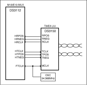
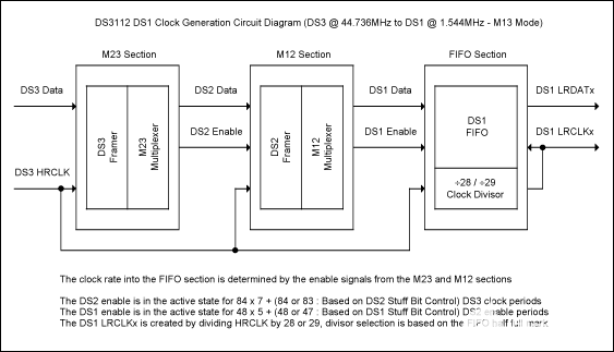
Figure 1. Transmit clock diagram.
The DS2(E2) transmit clocks are derived based on a fixed stuff rate, depending on the mode of the device. The stuff rate is expressed as a ratio of the number of times the stuff bit is not used to send payload data to the total number of stuff opportunities. The higher the ratio, the lower the effective clock frequency of the payload will be. The formulas for determining the DS2(E2) frequency are the following:
- DS2 Frequency = (672 - Stuff Rate) / 4760 x DS3 Frequency
- 672 is the number of DS2 payload bits in a DS3 frame.
- 4760 is the total number of bits in a DS3 frame.
- E2 Frequency = (378 - Stuff Rate) / 1536 x E3 Frequency
- 378 is the number of E2 payload bits in a E3 frame.
- 1536 is the total number of bits in a E3 frame.
Table 1. DS2(E2) Transmit Nominal Clock Rates Using Fixed Stuff Rates
| Mode | Stuff Rate | DS2(E2) With Exact DS3(E3) |
| DS3 C-Bit | 1/1 (100%) | DS2 = 6.306272MHz (-907ppm) |
| DS3 M13 | 7/18 (38.9%) | DS2 = 6.312016MHz (+2.53ppm) |
| G.747 C-Bit | 1/1 (100%) | DS2 = 6.306272MHz (-907ppm) |
| G.747 M13 | 7/18 (38.9%) | DS2 = 6.312016MHz (+2.53ppm) |
| E3 | 1/2 (50%) | E2 = 8.446562MHz (-170ppm) |
The minimum and maximum DS2(E2) clock frequencies using the fixed stuffing can be computed using the minimum and maximum DS3(E3) clock frequencies, which are ±20ppm. The results are in the following table.
Table 2. DS2(E2) Transmit Absolute Min and Max Clock Rates
| Mode | CLK | Min MHz | Max MHz |
| DS3 C-Bit | DS2 | 6.306146 (-927ppm) | 6.306398 (-887ppm) |
| DS3 M13 | DS2 | 6.311889 (-17.6ppm) | 6.312142 (+22.5ppm) |
| G.747 C-Bit | DS2 | 6.306146 (-927ppm) | 6.306398 (-887ppm) |
| G.747 M13 | DS2 | 6.311889 (-17.6ppm) | 6.312142 (+22.5ppm) |
| E3 | E2 | 8.446393 (-190ppm) | 8.446731 (-150ppm) |
Referencing the simple transmit clock diagram, the DS1(E1) port will use a stuff bit in the DS2(E2) frame to send an extra data bit when the FIFO is more than half full. The FIFO is emptied using the internal DS1(E1) clock, which is decoupled from the external DS1(E1) clock by the FIFO. On average, the internal clock is the same frequency as the external clock since the level in the FIFO is used to generate the internal clock, keeping the FIFO close to half full. The input DS1(E1) clock can have lots of jitter and can be bursty.
The DS1(E1) clock frequency has a maximum range determined by the amount of stuffing. The stuffing ratio can be from 0% to 100%. The formulas for determining the DS1(E1) maximum and minimum frequencies are given below:
Table 3. DS1(E1) Clock Rate Formulas
| Mode | DS1(E1) Frequency Formula |
| DS3 C-Bit | DS1 Frequency = (288 - Stuff Rate) / 1176 x DS2 Frequency |
| DS3 M13 | DS1 Frequency = (288 - Stuff Rate) / 1176 x DS2 Frequency |
| G.747 C-Bit | E1 Frequency = (273 - Stuff Rate) / 840 x DS2 Frequency |
| G.747 M13 | E1 Frequency = (273 - Stuff Rate) / 840 x DS2 Frequency |
| E3 | E1 frequency = (206 - Stuff Rate) / 848 x E2 frequency |
The absolute minimum and maximum DS1(E1) clock frequencies can be transmitted using the minimum and maximum DS2(E2) clock frequencies by setting the DS1(E1) stuff rate to 0% and 100%. The results are in the following table:
Table 4. DS1(E1) Absolute Transmit Min and Max Clock Rates
| Mode | CLK | Min MHz (100% Stuffing With Minimum DS2(E2)) |
Max MHz (0% Stuffing With Maximum DS2(E2)) |
| DS3 C-Bit | DS1 | 1.539000 (-3238ppm) | 1.544424 (+275ppm) |
| DS3 M13 | DS1 | 1.540402 (-2331ppm) | 1.545831 (+1186ppm) |
| G.747 C-Bit | E1 | 2.041990 (-2935ppm) | 2.049579 (+771ppm) |
| G.747 M13 | E1 | 2.043850 (-2026ppm) | 2.051446 (+1683ppm) |
| E3 | E1 | 2.041876 (-2990ppm) | 2.051918 (+1913ppm) |
The real minimum and maximum DS1(E1) clock frequencies that can be transmitted reverse the minimum and maximum DS2(E2) clock frequencies so that the maximum DS1(E1) clock frequency is set by the minimum DS2(E2) clock frequency with 0% stuffing. The results are in the following table:
Table 5. DS1(E1) Real Transmit Min and Max Clock Rates
| Mode | CLK | Min MHz (100% Stuffing With Minimum DS2(E2)) |
Max MHz (0% Stuffing With Maximum DS2(E2)) |
| DS3 C-Bit | DS1 | 1.539062 (-3198ppm) | 1.544362 (+235ppm) |
| DS3 M13 | DS1 | 1.540463 (-2291ppm) | 1.545769 (+1145ppm) |
| G.747 C-Bit | E1 | 2.042072 (-2895ppm) | 2.049497 (+731ppm) |
| G.747 M13 | E1 | 2.043932 (-1986ppm) | 2.051364 (+1643ppm) |
| E3 | E1 | 2.041957 (-2950ppm) | 2.051836 (+1873ppm) |
DS1(E1) Input Clocks
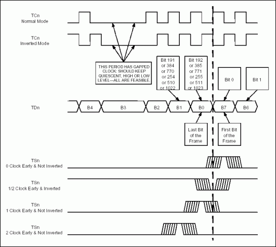
The DS3112 samples the DS1(E1) input clocks using the DS3(E3) clock and detects the low to high transition that is used to enable the internal high-speed system clock for one clock period. This sampling eliminates having more clock domains in the chip than is necessary. The associated DS1(E1) data is sampled by the high-speed system clock after the low to high edge is detected on the DS1(E1) clock input.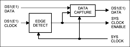
Figure 2. DS1(E1) Input clock sampling.
Receive Clocks
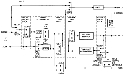
On the receive side, the DS3(E3) clock is supplied and the DS2(E2) and DS1(E1) clock frequencies are derived from it based on C-bit stuffing codes embedded in the overhead. The DS1(E1) clocks are generated using a DLL for each DS1(E1) port. There is an option of using an external common receive DS1(E1) clock, but that is beyond the scope of this application note. The DS3(E3), DS2(E2) and DS1(E1) clock frequencies are exactly the same as those transmitted at the at the source, when averaged. Each of the 16 to 28 DS1(E1) transmit clocks can be different, and each clock frequency will be recreated at the receiver where the signal is demutiplexed.
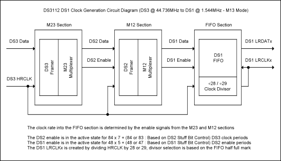
Figure 3. Receive clock diagram.
DS2(E2) Internal Clocks
The clock frequency formulas given for the transmit clocks apply to the receive clocks also. The DS2(E2) clocks are determined by the equipment that generated the format. Even though their tolerances should be ±30ppm, they can be at extremes depending on the stuffing rates of 0% to 100%. Note that DS2 minimum frequency is the same as the DS2 frequency in DS3 C-bit mode. The following table lists the absolute worst case DS2(E2) internal clocks based on the DS3(E3) minimum and maximum frequencies and a stuff rate of 0% and 100%:Table 6. DS2(E2) Receive Clock Frequencies at the Extreme Range Possible
| CLK | Min MHz | Max MHz |
| DS2 | 6.306146 (-927ppm) | 6.315797 (+602ppm) |
| E2 | 8.435206 (-1514ppm) | 8.457919 (+1174ppm) |
DS1(E1) Internal Clocks
The DS1(E1) clocks are derived from the DS2(E2) clocks and the C-bit stuff codes in the DS2(E2) overhead. The absolute worst case DS1(E1) clocks that could be used to put data into the receive FIFO are based on the absolute worst case DS2(E2) clocks and 0% and 100% stuffing and are listed in the following table:Table 7. DS1(E1) Receive Clock Frequencies at the Extreme Range Possible
| Mode | Min MHz | Max MHz |
| DS3 C-Bit | 1.539000 (-3238ppm) | 1.546726 (+1765ppm) |
| DS3 M13 | 2.041990 (-2934ppm) | 2.052634 (+2262ppm) |
| E3 | 2.039171 (-4311ppm) | 2.054636 (+3240ppm) |
The following table lists the internal DS1(E1) clock ranges based on the DS2(E2) industry specified clock frequency range of ±30ppm and the stuff rates of 0% and 100%:
Table 8. DS1(E1) Receive Clock Frequency Range Given DS2(E2) ±30ppm
| Mode | Min MHz | Max MHz |
| DS3 C-Bit | 1.540382 (-2343ppm) | 1.545842 (+1193ppm) |
| DS3 M13 | 2.043824 (-2039ppm) | 2.051462 (+1690ppm) |
| E3 | 2.042203 (-2830ppm) | 2.052288 (+2094ppm) |
DS1(E1) Output Clocks
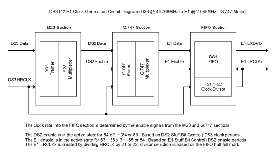
The DS1(E1) output clocks are created by dividing the DS3(E3) clock by one of two possible integers. The divisors to the DS1 clock are 29 and 28, the divisors for E1 are 17 and 16, and the divisors for G.747 are 22 and 21. One of the divisors is selected depending on whether the FIFO is more than half full or less than half full. When the FIFO is more than half full, the smaller divisor is used to empty the FIFO faster. The DS1(E1) output clocks will switch between two frequencies to recreate the average clock frequency at the transmitter.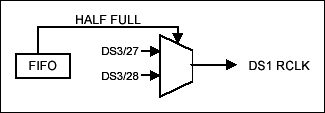
Figure 4. DS1 DLL.
The DS1(E1) clock rates switch from the following frequencies:
Table 9. DS1(E1) Clock Frequencies From DLL Output
| Mode | RCLK | Divisor | DS1(E1) Frequency |
| DS3 | DS1 Min | DS3/29 | 1.542621 (-893ppm) |
| DS3 | DS1 Max | DS3/28 | 1.597714 (+3489ppm) |
| G.747 | E1 Min | DS3/22 | 2.033455 (-7102ppm) |
| G.747 | E1 Max | DS3/21 | 2.130286 (+40179ppm) |
| E3 | E1 Min | E3/17 | 2.021647 (-12867ppm) |
| E3 | E1 Max | E3/16 | 2.148000 (+48828ppm) |
Reference
Table 10. Telecom Frequencies and Tolerances| Signal | Tolerance | Minimum MHz | Typical MHz | Maximum MHz |
| DS3 | ±20ppm | 44.735106 | 44.736000 | 44.736894 |
| DS2 | ±30ppm | 6.311811 | 6.312000 | 6.312189 |
| DS1 | ±50ppm | 1.543923 | 1.544000 | 1.544077 |
| E3 | ±20ppm | 34.367313 | 34.368000 | 34.368687 |
| E2 | ±30ppm | 8.447747 | 8.448000 | 8.448253 |
| E1 | ±50ppm | 2.047898 | 2.048000 | 2.048102 |
 電子發(fā)燒友App












評(píng)論