| Resolution (Bits) | 10 |
| Number of DAC channels (#) | 1 |
| Interface type | SPI |
| Output type | Buffered Voltage |
| Settling time (μs) | 12.5 |
| Features | Low Power |
| Reference type | Ext |
| Architecture | String |
| Rating | Catalog |
| Output range (Max) (mA/V) | 5.1 |
| Output range (Min) (mA/V) | 0 |
| Operating temperature range (C) | 0 to 70, -40 to 85 |
- 10-Bit CMOS Voltage Output DAC in an 8-Terminal Package
- 5V Single Supply Operation
- 3-Wire Serial Interface
- High-Impedance Reference Inputs
- Voltage Output Range: 2 Times the Reference Input Voltage
- Internal Power-On Reset
- Low Power Consumption: 1.75mW Max
- Update Rate of 1.21MHz
- Settling Time to 0.5LSB: 12.5μs Typ
- Monotonic Over Temperature
- Pin-Compatible With the Maxim MAX515
- APPLICATIONS
- Battery-Powered Test Instruments
- Digital Offset and Gain Adjustment
- Battery Operated/Remote Industrial Controls
- Machine and Motion Control Devices
- Cellular Telephones
SPI, QSPI are trademarks of Motorola, Inc.
Microwire is a trademark of National Semiconductor Corporation.
All other trademarks are the property of their respective owners.
The TLC5615 is a 10-bit voltage output digital-to-analog converter (DAC) with a buffered reference input (high impedance). The DAC has an output voltage range that is two times the reference voltage, and the DAC is monotonic. The device is simple to use, running from a single supply of 5V. A power-on-reset function is incorporated to ensure repeatable start-up conditions.
Digital control of the TLC5615 is over a three-wire serial bus that is CMOS compatible and easily interfaced to industry standard microprocessor and microcontroller devices. The device receives a 16-bit data word to produce the analog output. The digital inputs feature Schmitt triggers for high noise immunity. Digital communication protocols include the SPI?, QSPI?, and Microwire? standards.
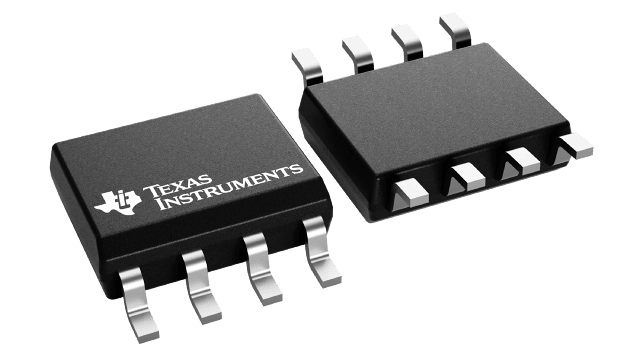
The 8-terminal small-outline D package allows digital control of analog functions in space-critical applications. The TLC5615C is characterized for operation from 0°C to +70°C. The TLC5615I is characterized for operation from -40°C to +85°C.


