| Resolution (Bits) | 12 |
| Number of DAC channels (#) | 2 |
| Interface type | SPI |
| Output type | Buffered Voltage |
| Settling time (μs) | 3 |
| Reference type | Ext |
| Architecture | String |
| Rating | HiRel Enhanced Product |
| Output range (Max) (mA/V) | 5.1 |
| Output range (Min) (mA/V) | 0 |
| Operating temperature range (C) | -55 to 125 |
- Controlled Baseline
- One Assembly/Test Site, One Fabrication Site
- Extended Temperature Performance of –55°C to 125°C
- Enhanced Diminishing Manufacturing Sources (DMS) Support
- Enhanced Product-Change Notification
- Qualification Pedigree

- Dual 12-Bit Voltage Output DAC
- Programmable Settling Time
- 3 μs in Fast Mode
- 10 μs in Slow Mode
- Compatible With TMS320 and SPI Serial Ports
- Differential Nonlinearity <0.5 LSB Typ
- Monotonic Over Temperature
- Direct Replacement for TLC5618A
- applications
- Digital Servo Control Loops
- Digital Offset and Gain Adjustment
- Industrial Process Control
- Machine and Motion Control Devices
- Mass Storage Devices
 Component qualification in accordance with JEDEC and industry standards to ensure reliable operation over an extended temperature range. This includes, but is not limited to, Highly Accelerated Stress Test (HAST) or biased 85/85, temperature cycle, autoclave or unbiased HAST, electromigration, bond intermetallic life, and mold compound life. Such qualification testing should not be viewed as justifying use of this component beyond specified performance and environmental limits.
SPI and QSPI are trademarks of Motorola, Inc.
Microwire is a trademark of National Semiconductor Corporation.
The TLV5618A is a dual 12-bit voltage output DAC with a flexible 3-wire serial interface. The serial interface is compatible with TMS320, SPI?, QSPI?, and Microwire? serial ports. It is programmed with a 16-bit serial string containing 4 control and 12 data bits.
The resistor string output voltage is buffered by an x2 gain rail-to-rail output buffer. The buffer features a Class-AB output stage to improve stability and reduce settling time. The programmable settling time of the DAC allows the designer to optimize speed versus power dissipation.
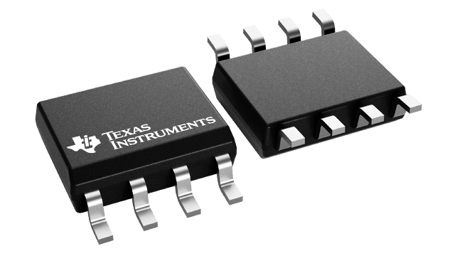
Implemented with a CMOS process, the device is designed for single supply operation from 2.7 V to 5.5 V. It is available in an 8-pin SOIC package.
The TLV5618AM is characterized for operation from ?55°C to 125°C.


