| Resolution (Bits) | 16 |
| Number of DAC channels (#) | 4 |
| Interface type | Parallel |
| Output type | Buffered Voltage |
| Settling time (μs) | 8 |
| Reference type | Ext |
| Architecture | String |
| Rating | Catalog |
| Output range (Max) (mA/V) | 5.5 |
| Output range (Min) (mA/V) | 0 |
| Operating temperature range (C) | -40 to 105 |
- Single Supply: +2.7 V to +5.5 V
- Micropower Operation: 950 μA @ 5 V
- Rail-To-Rail Voltage Output
- Ultralow Crosstalk: –110 dB
- Settling Time: 10 μs To ±0.003% FSR
- 16-Bit Monotonic
- Offset Error: ±0.3 mV
- Gain Error: ±1 mV
- Total Error: ±3 mV
- Per-Channel VREF+, VREF–, VFB Pins
- Logic Compatible: +1.8 V to +5.5 V
- Readback Capability
- Double Buffered Inputs
- Simultaneous or Sequential Update
- Schmitt-Triggered Digital Inputs
- Hardware Reset
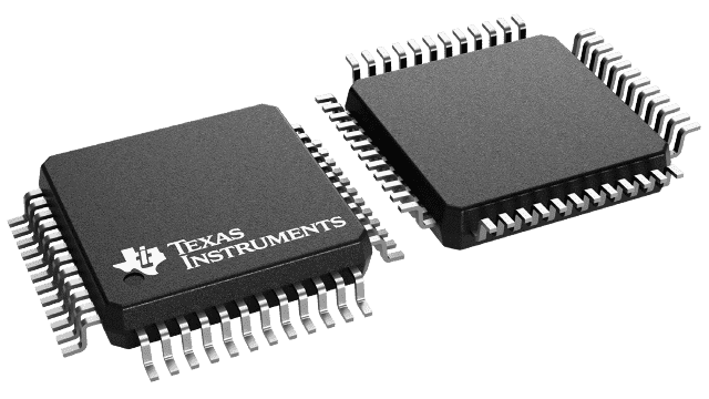
- 48-Lead TQFP Package
- APPLICATIONS
- Process Control
- Data Acquisition Systems
- Closed-Loop Servo Control
- PC Peripherals
- Optical Networking
The DAC8544 is a low-power, quad-channel, 16-bit, voltage output DAC. Its on-chip precision output amplifier allows rail-to-rail voltage swing to be achieved at the output. The DAC8544 is 16-bit monotonic and offers exceptional absolute accuracy with ultralow crosstalk. The DAC8544 uses a 16-bit parallel interface and features additional power-down function pins as well as hardware-enabled, synchronous DAC updating and reset capability.
The DAC8544 requires an external reference voltage to set the output range of the DAC. The device incorporates a power-on-reset circuit that ensures that the DAC outputs power up at zero volt and remains there until a valid write takes place. In addition, the DAC8544 contains a power-down feature, accessed via PD\ pin, that reduces the current consumption of the device to 400 nA at 5 V. The power consumption is typically under 5 mW at VDD = 5 V.
The DAC8544 is available in a 48-lead TQFP package with an operating temperature range of ?40°C to +105°C.


