| Resolution (Bits) | 14 |
| Number of DAC channels (#) | 4 |
| Interface type | SPI |
| Output type | Buffered Voltage |
| Settling time (μs) | 8 |
| Reference type | Ext, Int |
| Architecture | String |
| Rating | Catalog |
| Output range (Max) (mA/V) | 5.5 |
| Output range (Min) (mA/V) | 0 |
| Operating temperature range (C) | -40 to 105 |
- Relative Accuracy: 1LSB
- Glitch Energy: 0.15nV-s
- Internal Reference:
- 2.5V Reference Voltage (enabled by default)
- 0.004% Initial Accuracy (typ)
- 2ppm/°C Temperature Drift (typ)
- 5ppm/°C Temperature Drift (max)
- 20mA Sink/Source Capability
- Power-On Reset to Zero-Scale
- Ultra-Low Power Operation: 1mA at 5V
- Wide Power Supply Range: +2.7V to +5.5V
- 14-Bit Monotonic Over Temperature Range
- Settling Time: 10μs to ±0.006% Full-Scale Range (FSR)
- Low-Power Serial Interface with Schmitt-Triggered Inputs: Up to 50MHz
- On-Chip Output Buffer Amplifier with Rail-to-Rail Operation
- 1.8V to 5.5V Logic Compatibility
- Temperature Range: –40°C to +105°C
- APPLICATIONS
- Portable Instrumentation
- Closed-Loop Servo-Control
- Process Control, PLCs
- Data Acquisition Systems
- Programmable Attenuation
- PC Peripherals
All other trademarks are the property of their respective owners
The DAC8164 is a low-power, voltage-output, four-channel, 14-bit digital-to-analog converter (DAC). The device includes a 2.5V, 2ppm/°C internal reference (enabled by default), giving a full-scale output voltage range of 2.5V. The internal reference has an initial accuracy of 0.004% and can source up to 20mA at the VREFH/VREFOUT pin. The device is monotonic, provides very good linearity, and minimizes undesired code-to-code transient voltages (glitch). The DAC8164 uses a versatile 3-wire serial interface that operates at clock rates up to 50MHz. The interface is compatible with standard SPI, QSPI, Microwire, and digital signal processor (DSP) interfaces.
The DAC8164 incorporates a power-on-reset circuit that ensures the DAC output powers up at zero-scale and remains there until a valid code is written to the device. The device contains a power-down feature, accessed over the serial interface, that reduces the current consumption of the device to 1.3μA at 5V. Power consumption is 2.6mW at 3V, reducing to 1.4μW in power-down mode. The low power consumption, internal reference, and small footprint make this device ideal for portable, battery-operated equipment.
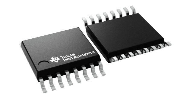
The DAC8164 is drop-in and functionally compatible with the DAC7564 and DAC8564, and functionally compatible with the DAC7565, DAC8165 and DAC8565. All these devices are available in a TSSOP-16 package.


