| Architecture | Fixed Gain/Buffer |
| Number of channels (#) | 1 |
| Total supply voltage (Min) (+5V=5, +/-5V=10) | 8 |
| Total supply voltage (Max) (+5V=5, +/-5V=10) | 12 |
| GBW (Typ) (MHz) | 650 |
| BW @ Acl (MHz) | 650 |
| Acl, min spec gain (V/V) | 1 |
| Slew rate (Typ) (V/us) | 3000 |
| Vn at flatband (Typ) (nV/rtHz) | 9.3 |
| Iq per channel (Typ) (mA) | 11.5 |
| Vos (offset voltage @ 25 C) (Max) (mV) | 7 |
| Rating | Catalog |
| Operating temperature range (C) | -40 to 85 |
| Input bias current (Max) (pA) | 15000000 |
| Offset drift (Typ) (uV/C) | 35 |
| Output current (Typ) (mA) | 90 |
| 2nd harmonic (dBc) | 62 |
| 3rd harmonic (dBc) | 78 |
| Frequency of harmonic distortion measurement (MHz) | 10 |
- Wideband operation
- AV = +1, VO = 0.5 VPP 650 MHz
- AV = +2, VO = 0.5 VPP 450 MHz
- AV = +2, VO = 2 VPP 400 MHz
- High output current ±90 mA
- Very low distortion
- 2nd/3rd harmonics (10 MHz, RL = 100?): ?62/?78dBc
- Differential gain/Differential phase: 0.02%/0.02°
- Low noise 2.3nV/√Hz
- High slew rate 3000 V/μs
- Supply current 11.5 mA
All trademarks are the property of their respective owners.
The LMH6704 is a very wideband, DC coupled selectable gain buffer designed specifically for wide dynamic range systems requiring exceptional signal fidelity. The LMH6704 includes on chip feedback and gain set resistors, simplifying PCB layout while providing user selectable gains of +1, +2 and ?1 V/V. The LMH6704 provides a disable pin, which places the amplifier in a high output impedance, low power mode. The Disable pin may be allowed to float high.
With a 650 MHz Small Signal Bandwidth (AV = +1), full power gain flatness to 200 MHz, and excellent Differential Gain and Phase, the LMH6704 is optimized for video applications. High resolution video systems will benefit from the LMH6704 ability to drive multiple video loads at low levels of differential gain or differential phase distortion.
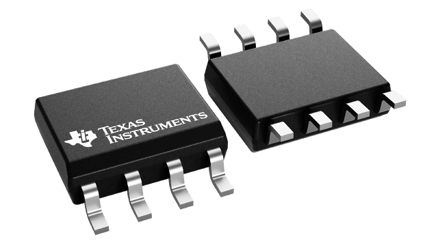
The LMH6704 is constructed with proprietary high speed complementary bipolar process using proven current feedback circuit architectures. It is available in 8 Pin SOIC and 6 Pin SOT-23 packages.


