Abstract: This power-supply sequencer senses a loss of the main supply voltage and, by controlling the two FETs, automatically switches the load to the secondary (backup) supply.
The Figure 1 circuit provides a "diode-OR" function for applications that must switch automatically between the main and backup supply voltages. Such applications include battery-backed memory supplies and any battery-operated device with a wall-adapter connection.
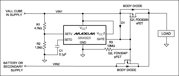
Figure 1. This power-supply sequencer senses a loss of the main supply voltage and, by controlling the two FETs, automatically switches the load to the secondary (backup) supply.
For example, a battery-backed SRAM circuit (nonvolatile memory module) requires at least two power sources: a high-current active path for the SRAM memory (VIN1), and a low-current standby supply (VIN2) that preserves memory contents when the main supply is removed. The conventional diode-OR connection shown in Figure 2 presents a problem in either path. In the VIN1 path, a diode drop can throw the supply voltage out of tolerance—3.3V ±10% has a minimum of 2.97V, so a typical diode drop (0.6V) places VIN1 outside the ±10% limit. The tolerance issue is even worse for memory ICs with lower voltage power supplies.
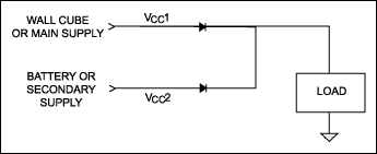
Figure 2. For less critical applications, this conventional "diode-OR" connection performs the same function as that of Figure 1.
On the standby side (VIN2), we want the lowest possible voltage drop to maximize the useful life of the standby source (whether battery, SuperCap?, or other voltage source). A drop of 0.6V, however, is approximately 15% of the output of a fully charged (4.1V) Li+ battery. Schottky diodes improve the situation somewhat, reducing the forward drop to a range of 0.3V to 0.5V, but substituting FETs for the diodes reduces the drop to nearly 0.1V. To create a "FET-ORed" supply with low forward drops, place a FET in each power path as shown in Figure 1. Both FETs are controlled by the power-supply sequencer U1.
You can decrease the losses on VIN1 and VIN2 to less than 50mV each by using an FDC633N transistor (Fairchild) for the VIN1 path and an FDN304P for the VIN2 path. Q1 was selected for its current-handling capabilities and low RDS(ON). Q2 was selected for low VGS (down to 1.8V—the equivalent of two depleted AA cells at 0.9V each) and low RDS(ON).
Both FETs are installed backwards to reverse-bias their body diodes and thereby prevent excessive current flow while providing a smoother transition from one source to the other.
U1 acts as a source detector and debouncer for the wall adapter. The device monitors VIN1 with a programmable delay (use MAX6819 for a typical fixed 200ms delay) to insure that battery power is not switched off until the wall supply is stable at or above U1's trip voltage.
Without D1, note that VIN2 could be back-driven by VIN1 (less the body-diode drop of Q1) during U1's timeout delay period. To prevent that problem, D1 drives Q2 off as power is applied from the primary source (VIN1).
U1's internal charge pump creates the GATE output that fully enhances Q1 and biases Q2 off. This output is approximately VCC2 + 5.5V (see Figure 3). R3 was added to drive the GATE signal more rapidly to ground, thereby assisting the turn-on of Q2 when VIN1 is removed. R3 should be as large as possible, because loading the GATE output resistively adds load current and reduces the gate-drive capability. (For proper operation, this circuit assumes the amplitude of VIN2 is less than that of VIN1.)
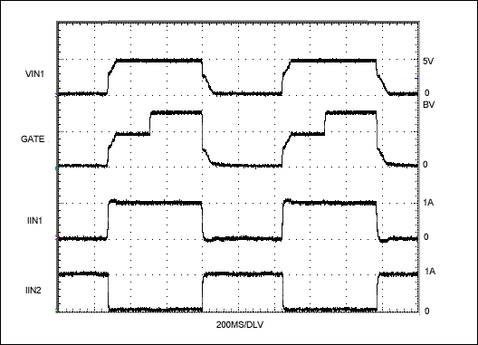
Figure 3. These waveforms illustrate performance of the Figure 1 circuit operating with a 1A load (VIN2 = 3V).
A similar article appeared in the March 2, 2006 edition of Electronic Design.
The Figure 1 circuit provides a "diode-OR" function for applications that must switch automatically between the main and backup supply voltages. Such applications include battery-backed memory supplies and any battery-operated device with a wall-adapter connection.

Figure 1. This power-supply sequencer senses a loss of the main supply voltage and, by controlling the two FETs, automatically switches the load to the secondary (backup) supply.
For example, a battery-backed SRAM circuit (nonvolatile memory module) requires at least two power sources: a high-current active path for the SRAM memory (VIN1), and a low-current standby supply (VIN2) that preserves memory contents when the main supply is removed. The conventional diode-OR connection shown in Figure 2 presents a problem in either path. In the VIN1 path, a diode drop can throw the supply voltage out of tolerance—3.3V ±10% has a minimum of 2.97V, so a typical diode drop (0.6V) places VIN1 outside the ±10% limit. The tolerance issue is even worse for memory ICs with lower voltage power supplies.

Figure 2. For less critical applications, this conventional "diode-OR" connection performs the same function as that of Figure 1.
On the standby side (VIN2), we want the lowest possible voltage drop to maximize the useful life of the standby source (whether battery, SuperCap?, or other voltage source). A drop of 0.6V, however, is approximately 15% of the output of a fully charged (4.1V) Li+ battery. Schottky diodes improve the situation somewhat, reducing the forward drop to a range of 0.3V to 0.5V, but substituting FETs for the diodes reduces the drop to nearly 0.1V. To create a "FET-ORed" supply with low forward drops, place a FET in each power path as shown in Figure 1. Both FETs are controlled by the power-supply sequencer U1.
You can decrease the losses on VIN1 and VIN2 to less than 50mV each by using an FDC633N transistor (Fairchild) for the VIN1 path and an FDN304P for the VIN2 path. Q1 was selected for its current-handling capabilities and low RDS(ON). Q2 was selected for low VGS (down to 1.8V—the equivalent of two depleted AA cells at 0.9V each) and low RDS(ON).
Both FETs are installed backwards to reverse-bias their body diodes and thereby prevent excessive current flow while providing a smoother transition from one source to the other.
U1 acts as a source detector and debouncer for the wall adapter. The device monitors VIN1 with a programmable delay (use MAX6819 for a typical fixed 200ms delay) to insure that battery power is not switched off until the wall supply is stable at or above U1's trip voltage.
Without D1, note that VIN2 could be back-driven by VIN1 (less the body-diode drop of Q1) during U1's timeout delay period. To prevent that problem, D1 drives Q2 off as power is applied from the primary source (VIN1).
U1's internal charge pump creates the GATE output that fully enhances Q1 and biases Q2 off. This output is approximately VCC2 + 5.5V (see Figure 3). R3 was added to drive the GATE signal more rapidly to ground, thereby assisting the turn-on of Q2 when VIN1 is removed. R3 should be as large as possible, because loading the GATE output resistively adds load current and reduces the gate-drive capability. (For proper operation, this circuit assumes the amplitude of VIN2 is less than that of VIN1.)

Figure 3. These waveforms illustrate performance of the Figure 1 circuit operating with a 1A load (VIN2 = 3V).
A similar article appeared in the March 2, 2006 edition of Electronic Design.
 電子發燒友App







評論