Pushing the Limits of Packaging
Packaging of microcontrollers plays a key role in the miniaturization of a system. The tradeoff of the choice of peripherals on the die, the pad count and the die size all limit the ability to reduce the size of the microcontroller, but nevertheless help reduce the overall size of the end equipment. Thermal issues are also important to consider as microcontrollers get smaller in size. With more transistors on a small die, running at higher frequencies, the power dissipation is a key consideration. While reducing the voltage and gating the different peripherals so that unused elements are not consuming power can reduce the overall thermal load, the excess heat generated must then be efficiently removed or the microcontroller will degrade and ultimately fail. This is a key reliability issue that has to be considered in miniaturizing the microcontroller system. This is where the tradeoff of pins versus size comes in. Additional pins on a package can be used to connect to thermal vias to take excess heat away from the microcontroller and other devices that may be sensitive to elevated temperatures such as a wireless interface. While the latest chip-scale packaging can reduce the overall footprint of a device with a given functionality, reducing the area taken up by a quarter, the opportunity to integrate more peripherals into a device and have more pins for thermal dissipation may be more important. The designer also has to be aware of the aim of miniaturization. An ARM 32-bit core, such as the Cortex-M0+ or even the M4, is less than a square millimeter of silicon – the size of the die is determined more by the amount of memory on chip and, vital for the packaging consideration, the peripherals that need to connect to the outside world. The smallest M0 devices, such as Freescale’s Kinetis KL02, can be as small as 1.9 x 2.0 mm in a chip-scale package that is barely larger than the die itself. At less than 4 square millimeters, this occupies twenty-five percent less PCB area than ball grid array or LGA packages but provides sixty percent more GPIO with up to twenty-eight lines. This move, almost 'silicon dust', allows designers to dramatically reduce their board size without compromising the performance, feature integration and power consumption of the end products.?
Figure 1: The Kinetis KL02 family in chip-scale packaging provides a full microcontroller in a few square millimeters.?Power consumption and thermal considerations are key at this size, and there are many things that can be done on the chip to reduce overall power dissipation and allow for a smaller package. The core runs at 48 MHz, helping to keep the power down over the whole -40°C to +105°C temperature range and allows the devices to be used in as many different environments as possible. There are also multiple low-power modes such as a new compute mode that reduces dynamic power by placing peripherals in an asynchronous stop mode. The Low-Power UART (LPUART), SPI, I2C, data converters, low-power timer and DMA engine all support a low-power mode operation where they operate without waking up the core. However, this does not necessarily reflect the actual use of silicon. Making many different versions of a microcontroller with a wide range of peripherals and memory options is actually expensive if separate masks are required. Instead, a single design with a superset of functions is implemented and manufactured, and only a specific set of features connected. This allows the silicon vendor to provide a wide range of products while minimizing the manufacturing costs and benefiting from economies of scale. The next stage of development has been to create a more flexible I/O configuration. Just as an internal bus matrix connects the peripherals, (as in the Atmel 4S family) so vendors are also introducing designs with a matrix that connects the I/O pins. This allows any peripheral to connect to any I/O pin, providing more flexibility for the vendor to deliver a family of pin-compatible devices where the same I/Os are always in the same place. As there is silicon to spare, this helps the system designer have a design with scalable performance without impacting on the overall size. All this means that the packaging technology is the key to the miniaturization of the microcontroller. Atmel has developed the SAM G51 series of Flash microcontrollers that is also based on the M4 core with floating point support. This also operates at a maximum speed of 48 MHz and features up to 256 Kbytes of Flash and up to 64 Kbytes of SRAM. The peripheral set includes one USART, two UARTs, two TWIs, one high-speed TWI, up to two SPIs, one three-channel general-purpose 16-bit timer, one RTT and one 8-channel, 12-bit ADC, greatly driving up the pin count requirements.?

Figure 2: The Atmel SAM G51 family of microcontrollers showing the range of package options.?This peripheral set allows the SAM G51 series to target a wide range of applications including consumer, industrial control, and PC peripherals with just two package types – a 49-ball WLCSP chip-scale package or a 100-lead LQFP package. At the same time, Atmel's SAM4S series is also based on the ARM Cortex-M4 processor core. It operates at higher maximum speed of 120 MHz and features up to 2048 Kbytes of Flash, with optional dual-bank implementation and cache memory, and up to 160 Kbytes of SRAM. The peripheral set includes a full-speed USB device port with embedded transceiver, a high-speed MCI for SDIO/SD/MMC, an external Bus interface with memory controller, two USARTs, two UARTs, two TWIs, three SPIs, one I2S, as well as one PWM timer, two three-channel general-purpose 16-bit timers (with stepper motor and quadrature decoder logic support), one RTC, one 12-bit ADC, one 12-bit DAC and one analog comparator. All of this brings even greater demands on the packaging and the pin count. The family has up to seventy-nine I/O lines with external interrupt capability (edge or level sensitivity), debouncing, glitch filtering and on-die series resistor termination, as well as three 32-bit Parallel Input/Output Controllers. This leads to a range of packages, from 100 leads down to 48 leads, but using the more traditional technologies: 100-lead packages
LQFP, 14 x 14 mm, pitch 0.5 mm TFBGA, 9 x 9 mm, pitch 0.8 mm VFBGA, 7 x 7 mm, pitch 0.65 mm
64-lead packages
LQFP, 10 x 10 mm, pitch 0.5 mm QFN, 9 x 9 mm, pitch 0.5 mm WLCSP, 4.42 x 3.42 mm, pitch 0.4 mm (SAM4S16/S8) WLCSP, 3.32 x 3.32 mm, pitch 0.4 mm (SAM4S4/S2)
48-lead packages
LQFP, 7 x 7 mm, pitch 0.5 mm QFN, 7 x 7 mm, pitch 0.5 mm
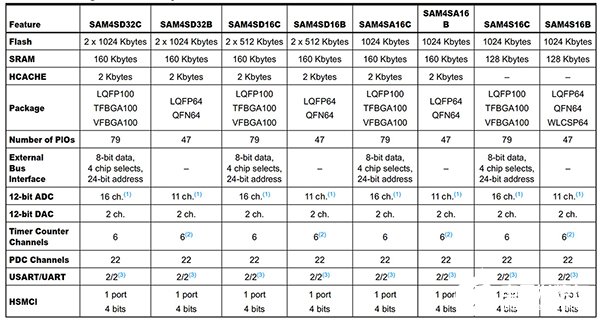
Figure 3: The Atmel SAM4S family has a much wider range of peripheral options leading to larger packages.?Future trends?New packaging technologies that stack die on top of each other in the same package also help to reduce the overall footprint. Instead of having a separate memory chip alongside the microcontroller, the microcontroller die is mounted on top of a memory die or large FPGA in one package. This approach, commonly called 2.5D, requires a silicon interposer and through silicon vias (TSVs) which is a relatively new technology that is now maturing and becoming more common. This is used in high-end devices that need larger amounts of memory that cannot be cost effectively integrated on a single die. Full 3D packaging sees multiple die stacked directly on top of each other; perhaps with I/O pads on the edges to allow interconnect between the different devices. While this has been a long-term aim of miniaturization, combining all the elements on a printed circuit board from the microcontroller to memory and wireless interface into one packaged device, it has yet to overcome a number of cost, reliability and thermal issues.?Conclusion?The wide range of microcontrollers from multiple vendors hides a strategy in the miniaturization of such devices. The range of packaging in different families from one vendor, all around the same core, demonstrates the complex tradeoff between footprint, peripheral mix, power, and system size. Further down the performance curve, 32-bit controllers with complex peripherals are now little more than a couple of square millimeters, becoming 'silicon dust' that permeates the Internet of Things.
破除封裝的限制
包裝微控制器起著一個系統的小型化的關鍵作用。在管芯的外圍設備的選擇的折衷,襯墊計數和芯片尺寸的所有限制,以減少微控制器的尺寸,但仍然有利于降低端設備的整體尺寸的能力。散熱問題也是需要考慮的微控制器獲得規模較小重要。與上一個小芯片更多的晶體管,運行在較高的頻率時,功耗是一個關鍵的考慮因素。同時降低了電壓門控和在不同的外設,使未使用的元件不消耗功率可以降低整體的熱負荷,產生的多余熱量必須再有效地去除或微控制器將降低并最終失敗。這是一個關鍵的可靠性問題,有在小型化的微控制器系統中加以考慮。這就是銷與大小的折衷用武之地。上一包的附加引腳可以用于連接到散熱通孔采取多余的熱量遠離微控制器和其他設備可以是在升高的溫度敏感諸如無線接口。而最新的芯片級封裝可以減少設備的整體尺寸與給定的功能,從而減少了四分之一占據的區域,有機會更多外設集成到一個設備,并有更多的引腳用于熱耗散可能更重要。設計者還必須知道的小型化的目的。
? ? ? 一個ARM 32位核,如在Cortex-M0 +或甚至在M4,小于硅的平方毫米 - 管芯的尺寸更受的存儲器芯片的數量,并且對于包裝考慮的重要決定,需要連接到外部世界的外設。最小M0設備,如飛思卡爾的Kinetis KL02,可以小如1.9×2.0毫米的芯片級封裝,僅比管芯本身大。在小于4平方毫米,這占用較少的百分之二十五的PCB面積比球柵陣列或LGA封裝,但提供的百分之六十以上的GPIO多達28行。此舉,幾乎是'硅塵“,使設計人員能夠大幅降低其電路板尺寸不影響性能,功能集成的終端產品和功耗。
飛思卡爾的Kinetis KL02系列圖1形象:Kinetis KL02系列的芯片級封裝提供了一個完整的微控制器在幾平方毫米。功率消耗和散熱的考慮是,在這個尺寸鍵,并且存在可以在芯片上完成,以降低整體功耗,并允許更小的封裝許多東西。核心運行在48兆赫,有助于保持掉電在整個-40°C到+ 105℃的溫度范圍內,并且允許設備在許多不同的環境中盡可能地使用。也有多個低功率模式,如新的計算模式,它使外圍設備異步停止模式降低動態功耗。低功耗UART(LPUART),SPI,I2C,數據轉換器,低功耗定時器和DMA引擎都支持,他們沒有醒來的核心操作低功率模式操作。然而,這并不一定反映實際使用的硅。如果單獨口罩都需要做許多不同版本的微控制器具有廣泛的外設和存儲器的選擇實際上是昂貴的。相反,隨著功能的一個超集的單個設計實現和制造,并且只有一組特定的連接的功能。這使得芯片供應商提供范圍廣泛的產品,同時最大限度地降低生產成本,并受益于規模經濟。發展的下一階段是創建一個更加靈活的I / O配置。只是作為一個內部總線矩陣連接的外圍設備,(如在愛特梅爾4S家族),所以廠商也引入設計與基質連接的I / O引腳。這允許任何外圍設備連接到任何的I / O引腳,為供應商提供了更大的靈活性,提供一個家庭的,其中相同的I / O是總是在同一個地方管腳兼容的設備。由于有硅不遺余力,這有助于系統設計有可伸縮的性能設計,而不會影響整體規模。這一切都意味著,封裝技術的關鍵是單片機的小型化。
Atmel公司已經開發出了SAM G51系列閃存微控制器也是基于對M4內核浮點支持。這也工作在48 MHz的最高速度,并具有高達256 KB的閃存和64 KB的SRAM的。該外設集包括一個USART,兩個UART,二TWIs,一臺高速TWI,高達2個SPI,一是三通道通用的16位定時器,一個RTT和一個8通道,12位ADC,大大哄抬引腳數的要求。
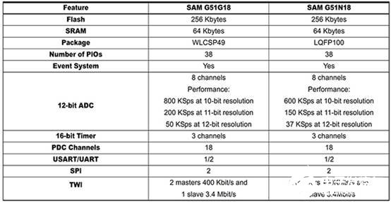
愛特梅爾SAM G51系列微控制器顯示封裝選擇的范圍:愛特梅爾SAM G51系列圖2圖像。該外設允許SAM G51系列針對廣泛的應用,包括消費電子,工業控制和PC外設只有兩種封裝類型 - 一個49引腳WLCSP芯片級封裝或100引腳LQFP封裝。與此同時,Atmel的SAM4S系列也基于ARM Cortex-M4處理器核心。它工作在120 MHz的更高的最高速度,并設有高達2048 KB的閃存,可選雙行執行與高速緩存,以及高達160字節的SRAM。外設集包括嵌入式收發器全速USB設備端口,高速MCI的SDIO / SD / MMC,內存控制器,兩個USART,兩個UART,二TWIs,三SPI的一I2S一個外部總線接口,還有一個PWM定時器,兩個三通道通用的16位定時器(帶步進電機和正交解碼器邏輯支持),一個RTC,一個12位ADC,一個12位DAC和一個模擬比較器。所有這一切都使在包裝和銷數更大的要求。該系列有多達79 I /外部中斷功能(邊緣或水平靈敏度),消除抖動,假信號過濾和管芯串聯電阻端接,以及三個32位并行輸入/輸出控制器O線。這導致了一系列的包,從100向下通往48引線,但使用更傳統的技術:100引線封裝
LQFP,14×14毫米,間距0.5毫米
TFBGA,9×9毫米,節距0.8毫米
VFBGA,7×7毫米,間距0.65毫米
64引腳封裝
LQFP,10×10毫米,間距0.5毫米
QFN,9×9毫米,間距0.5毫米
WLCSP,4.42 x3.42毫米,間距0.4毫米(SAM4S16 / S8)
WLCSP,3.32 x3.32毫米,間距0.4毫米(SAM4S4 / S2)
48引腳封裝
LQFP,7×7毫米,間距0.5毫米
QFN,7×7毫米,間距0.5毫米

愛特梅爾SAM4S系列圖3圖片:愛特梅爾SAM4S系列具有更廣泛的外設選項,導致更大的封裝。未來趨勢的新包裝技術,堆疊死在彼此的頂部在同一個包也有利于降低整體的足跡。代替具有沿著微控制器單獨的存儲器芯片,該微控制器芯片被安裝在一個封裝的存儲器芯片或大的FPGA的頂部。這種方法,通常稱為2.5D,需要一個硅中介層,并通過硅通孔(TSV),這是一個相對較新的技術,現在是成熟和變得越來越普遍。這是用在那些需要大容量內存,不能有效的成本在單一芯片上集成的高端設備。全3D包裝看到多個芯片堆疊直接在彼此頂部;或許與I /上邊緣O墊,以允許不同的設備之間的互連。盡管這是一個長期的目標小型化,結合從微控制器的內存和無線接口印刷電路板的所有元素融入其中封裝器件,它尚未攻克一批成本,可靠性和散熱問題的。結論廣泛來自多個供應商的微控制器隱藏在這種裝置的小型化的策略。包裝在不同的家庭從一個供應商的范圍內,所有周圍的相同的核心,顯示足跡,外設組合,功率和系統尺寸之間的復雜的平衡。再往下的性能曲線,32位控制器具有復雜的外設,現在多一點幾平方毫米以上,成為“硅塵”的滲透物聯網。
 電子發燒友App







評論