Abstract: Recently, the MAX555 has changed its package type from a 68-pin PLCC (Plastic Lead Chip Carrier) to a 64-pin TQFP (Thin Quad Flat Pack) package. To accommodate the package change in existing designs, this application note was created to provide helpful PCB layout guidelines for designers who have been developing systems based on the PLCC version of the MAX555 and are now required to make a quick and effortless transition from PLCC to TQFP.
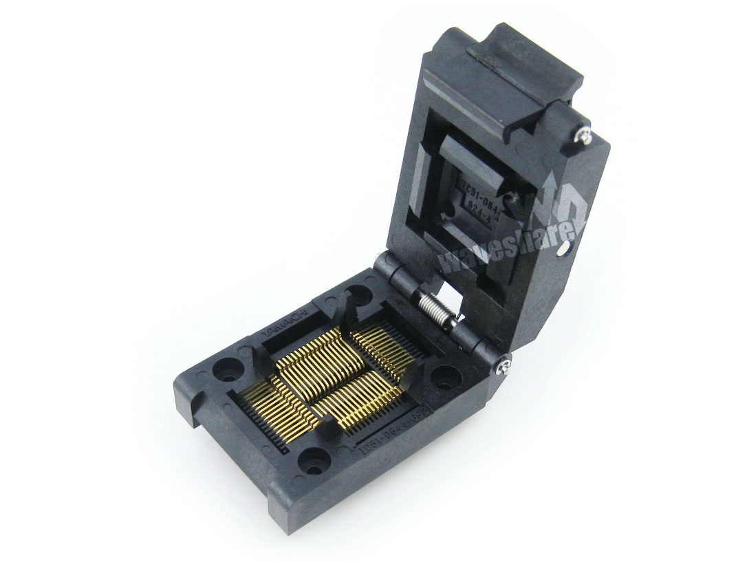
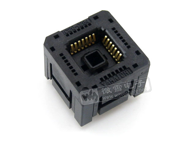
The MAX555 now has migrated from a 68-pin PLCC (Figure 1a) to a new 64-pin TQFP (Figure 1b) package with exposed paddle. This package change has not only helped to reduce the package size significantly, but also lowered the thermal resistance from 28°C/W to 25°C/W. However, the die orientation within the package has now changed from 'cavity-down' to 'cavity-up', causing the pinout to change.
Figure 1a. Old 68-pin PLCC pinout.
Figure 1b. New 64-pin TQFP pinout.
To ease the switch from PLCC to TQFP, this application note suggests means for modifying an existing PCB layout to adapt to the new package with minimal disruption.
Figure 2 illustrates the old PLCC package (a) on the left, and the new TQFP package (b) on the right, both to the same scale. It becomes immediately apparent that the new TQFP package is much smaller than the old PLCC package. This reduction in package size allows ample room to execute the necessary PCB trace adjustments to align the new pinout to the old pinout. Although each individual layout will have its unique aspects, the general method described and illustrated in this application note can be applied to individual circumstances.
Figure 2. PCB layout supports old 68-pin PLCC package (a). PCB layout changes suggested, to fit the 64-pin TQPF pinout into an existing 68-pin PLCC outline (b).
On an example PCB, designed to accommodate the PLCC package, the digital bus enters the digital-to-analog converter (DAC) on the top of the package (a). In this view, pin 1 is located at the top center of the package, with the analog outputs exiting on the left side of the package. All 50Ω ECL termination resistors are located adjacent to the input pins. The remaining two sides of the package are devoted to power and reference pins and their associated decoupling capacitors. Keep all power supply traces, ground traces, and bypass capacitor connections short to minimize the parasitic inductance.
On a PCB, designed to accommodate the new TQFP layout, the digital bus still approaches the top of the package (b). The location of pin 1 on the TQFP package however is in the lower right-hand corner. The digital inputs are routed to either an inner layer or to the bottom side of the board. They are routed under the TQFP package. It is important that a solid ground plane exists between the digital bus under the TQFP package and the topside traces. Such a ground plane supports heat dissipation and provides shielding to isolate the digital signals from the device. It is recommended that the traces routed beneath the TQFP package maintain the desired 50Ω transmission line impedance for optimum signal integrity. Running a power or ground plane on a layer adjacent to these traces supports controlling their impedance. Furthermore, clock signals should be routed as a differential pair, and be isolated from the digital bus traces by at least two trace widths to ensure a clean clock source.
The digital bus is then brought to the topside of the board through an array of vias, and routed to both the input pins of the TQFP package and the 50Ω termination resistors through short traces. Since the smaller TQFP package fits within the PLCC outline, these traces, vias and resistors fall within the PLCC dimensions, eliminating any layout impact on surrounding circuitry.
The reference circuitry bypass capacitors must be moved from the bottom edge of the PLCC package to the top edge of the TQFP package. Power supply decoupling capacitors remain on the right-hand side of the package and the analog outputs remain on the left side of the package. However, note that the order of the analog outputs is reversed. This reversal is corrected with a simple crossover (b) of the differential signals.
The thermal (or exposed) pad on the bottom of the TQFP package must be connected to AGND. Using multiple vias to connect this pad to the underlying ground promotes minimizing both its thermal resistance and ground connection impedance.
These suggested layout changes result in a preservation of the basic I/O buses to and from the DAC. ECL input signals can have extremely fast rise times and for satisfactory waveform fidelity, it is recommended that the electrical length of unmatched transmission lines is less than one fourth of the signal rise time. This will limit over- and under-shoot to less than 15%. For a rise time of 300ps, this suggests unmatched lines lengths of less than 1.5cm (0.6 inch). Both layouts illustrated in Figure 2 meet this requirement. All bypass capacitors, power and ground connections should be very short. Figures 2a and 2b depict trace lengths less than 2mm (0.08 inch). All these suggestions support optimizing the dynamic performance of the MAX555.
 電子發燒友App








評論